SNVS363E August 2005 – November 2015 LM5026
PRODUCTION DATA.
- 1 Features
- 2 Applications
- 3 Description
- 4 Revision History
- 5 Pin Configuration and Functions
- 6 Specifications
-
7 Detailed Description
- 7.1 Overview
- 7.2 Functional Block Diagram
- 7.3
Feature Description
- 7.3.1 High Voltage Start-Up Regulator
- 7.3.2 Line Undervoltage Detector
- 7.3.3 PWM Outputs
- 7.3.4 Gate Driver Outputs
- 7.3.5 PWM Comparator/Slope Compensation
- 7.3.6 Maximum Duty Cycle Clamp
- 7.3.7 Soft-Start / Soft-Stop
- 7.3.8 Current Sense and Current Limit
- 7.3.9 Overload Protection Timer
- 7.3.10 Oscillator and Sync Capability
- 7.3.11 Thermal Protection
- 7.4 Device Functional Modes
-
8 Application and Implementation
- 8.1 Application Information
- 8.2 Typical Application
- 9 Power Supply Recommendations
- 10Layout
- 11Device and Documentation Support
- 12Mechanical, Packaging, and Orderable Information
1 Features
- Current-Mode Control
- Internal 100-V Start-Up Bias Regulator
- 3-A Compound Main Gate Driver
- High Bandwidth Optocoupler Interface
- Programmable Line Undervoltage Lockout (UVLO) With Adjustable Hysteresis
- Versatile Dual Mode Overcurrent Protection With Hiccup Delay Timer
- Programmable Overlap or Deadtime between the Main and Active Clamp Outputs
- Programmable Maximum Duty Cycle Clamp
- Programmable Soft-Start
- Leading Edge Blanking
- Resistor Programmed 1-MHz Capable Oscillator
- Oscillator Sync I/O Capability
- Precision 5-V Reference
2 Applications
- Server Power Supplies
- 48-V Telecom Power Supplies
- High Efficiency DC–DC Power Supplies
3 Description
The LM5026 PWM controller contains all of the features necessary to implement power converters utilizing the active clamp and reset technique with current-mode control. With the active clamp technique, higher efficiencies and greater power densities can be realized compared to conventional catch winding or RDC clamp and reset techniques. Two control outputs are provided, the main power switch control (OUT_A) and the active clamp switch control (OUT_B). The device can be configured to control either a P-Channel or N-Channel clamp switch. The main gate driver features a compound configuration, consisting of both MOS and Bipolar devices, providing superior gate drive characteristics. The LM5026 can be configured to operate with bias voltages over a wide input range of 8 V to 100 V. Additional features include programmable maximum duty cycle, line undervoltage lockout, cycle-by-cycle current limit, hiccup mode fault operation with adjustable timeout delay, PWM slope compensation, soft-start, 1-MHz capable oscillator with synchronization input and output capability, precision reference, and thermal shutdown.
Device Information(1)
| PART NUMBER | PACKAGE | BODY SIZE (NOM) |
|---|---|---|
| LM5026 | WSON (16) | 5.00 mm × 5.00 mm |
| TSSOP (16) | 4.40 mm × 5.00 mm |
- For all available packages, see the orderable addendum at the end of the data sheet.
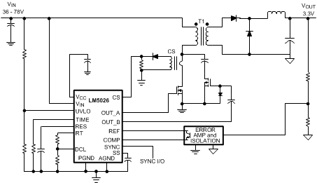
Typical Application Circuit
