SNVS293F December 2004 – August 2016 LM5025A
PRODUCTION DATA.
- 1 Features
- 2 Applications
- 3 Description
- 4 Revision History
- 5 Pin Configuration and Functions
- 6 Specifications
- 7 Detailed Description
- 8 Application and Implementation
- 9 Power Supply Recommendations
- 10Layout
- 11Device and Documentation Support
- 12Mechanical, Packaging, and Orderable Information
6 Specifications
6.1 Absolute Maximum Ratings
over operating free-air temperature range (unless otherwise noted)(1)(2)| MIN | MAX | UNIT | ||
|---|---|---|---|---|
| VIN to GND | –0.3 | 105 | V | |
| VCC to GND | –0.3 | 16 | V | |
| CS1, CS2 to GND | –0.3 | 1 | V | |
| All other inputs to GND | –0.3 | 7 | V | |
| Junction temperature, TJ | 150 | °C | ||
| Storage temperature, Tstg | –55 | 150 | °C | |
(1) Stresses beyond those listed under Absolute Maximum Ratings may cause permanent damage to the device. These are stress ratings only, which do not imply functional operation of the device at these or any other conditions beyond those indicated under Recommended Operating Conditions. Exposure to absolute-maximum-rated conditions for extended periods may affect device reliability.
(2) If Military/Aerospace specified devices are required, please contact the TI Sales Office/ Distributors for availability and specifications.
6.2 ESD Ratings
| VALUE | UNIT | |||
|---|---|---|---|---|
| V(ESD) | Electrostatic discharge | Human-body model (HBM)(1) | ±2000 | V |
(1) JEDEC document JEP155 states that 500-V HBM allows safe manufacturing with a standard ESD control process.
6.3 Recommended Operating Conditions
over operating free-air temperature range (unless otherwise noted)| MIN | MAX | UNIT | |
|---|---|---|---|
| VIN voltage | 13 | 90 | V |
| External voltage applied to VCC | 8 | 15 | V |
| Operating junction temperature | –40 | 125 | °C |
6.4 Thermal Information
| THERMAL METRIC(1) | LM5025A | UNIT | ||
|---|---|---|---|---|
| PW (TSSOP) | NHQ (WSON) | |||
| 16 PINS | 16 PINS | |||
| RθJA | Junction-to-ambient thermal resistance | 98.7 | 30 | °C/W |
| RθJC(top) | Junction-to-case (top) thermal resistance | 27.8 | 25.9 | °C/W |
| RθJB | Junction-to-board thermal resistance | 44.3 | 9.3 | °C/W |
| ψJT | Junction-to-top characterization parameter | 1.2 | 0.2 | °C/W |
| ψJB | Junction-to-board characterization parameter | 43.6 | 9.5 | °C/W |
| RθJC(bot) | Junction-to-case (bottom) thermal resistance | — | 2.3 | °C/W |
(1) For more information about traditional and new thermal metrics, see the Semiconductor and IC Package Thermal Metrics application report.
6.5 Electrical Characteristics
Typical limits are for TJ = 25°C, and minimum and maximum limits apply over the operating junction temperature range (–40°C to 125°C). VIN = 48 V, VCC = 10 V, RT = 31.3 kΩ, RSET = 27.4 kΩ) unless otherwise stated (1)| PARAMETER | TEST CONDITIONS | MIN | TYP | MAX | UNIT | ||
|---|---|---|---|---|---|---|---|
| START-UP REGULATOR | |||||||
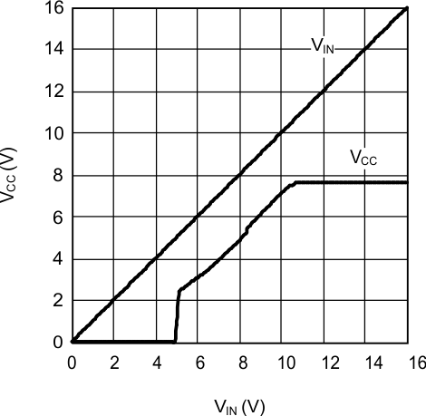
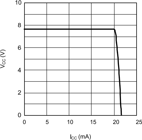
| VCC Reg | VCC regulation | No load | TJ = 25°C | 7.6 | V | ||
| TJ = Tlow to Thigh | 7.3 | 7.9 | |||||
| VCC current limit | See (2) | TJ = 25°C | 25 | mA | |||
| TJ = Tlow to Thigh | 20 | ||||||
| I-VIN | Start-up regulator leakage (external Vcc Supply) | VIN = 100 V | TJ = 25°C | 165 | µA | ||
| TJ = Tlow to Thigh | 500 | ||||||
| VCC SUPPLY | |||||||
| VCC undervoltage lockout voltage (positive going Vcc) | TJ = 25°C | VCC Reg - 120 mV | V | ||||
| TJ = Tlow to Thigh | VCC Reg - 220 mV |
||||||
| VCC undervoltage hysteresis | TJ = 25°C | 1.5 | V | ||||
| TJ = Tlow to Thigh | 1 | 2 | |||||
| VCC supply current (ICC) | Cgate = 0 | TJ = Tlow to Thigh | 4.2 | mA | |||
| REFERENCE SUPPLY | |||||||
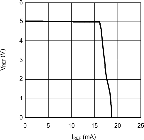
| VREF | Ref voltage | IREF = 0 mA | TJ = 25°C | 5 | V | ||
| TJ = Tlow to Thigh | 4.85 | 5.15 | |||||
| Ref voltage regulation | IREF = 0 to 10mA | TJ = 25°C | 25 | mV | |||
| TJ = Tlow to Thigh | 50 | ||||||
| Ref current limit | TJ = 25°C | 20 | mA | ||||
| TJ = Tlow to Thigh | 10 | ||||||
| CURRENT LIMIT | |||||||
| CS1 Prop | CS1 delay to output | CS1 Step from 0 to 0.6 V, Time to onset of OUT Transition (90%), Cgate = 0 |
40 | ns | |||
| CS2 Prop | CS2 delay to output | CS2 Step from 0 to 0.6 V, Time to onset of OUT Transition (90%), Cgate = 0 |
50 | ns | |||
| Cycle by cycle threshold voltage (CS1) | TJ = 25°C | 0.5 | V | ||||
| over full operating junction temperature | 0.45 | 0.55 | |||||
| Cycle skip threshold voltage (CS2) | Resets SS capacitor; auto restart | TJ = 25°C | 0.5 | V | |||
| TJ = Tlow to Thigh | 0.45 | 0.55 | |||||
| Leading edge blanking time (CS1) | 50 | ns | |||||
| CS1 sink impedance (clocked) | CS1 = 0.4 V | TJ = 25°C | 30 | Ω | |||
| TJ = Tlow to Thigh | 50 | ||||||
| CS1 sink impedance (post fault discharge) | CS1 = 0.6 V | TJ = 25°C | 15 | Ω | |||
| TJ = Tlow to Thigh | 30 | ||||||
| CS2 sink impedance (post fault discharge) | CS2 = 0.6 V | TJ = 25°C | 55 | Ω | |||
| TJ = Tlow to Thigh | 95 | ||||||
| CS1 and CS2 leakage current | CS = CS Threshold – 100 mV | TJ = Tlow to Thigh | 1 | µA | |||
| SOFT-START | |||||||
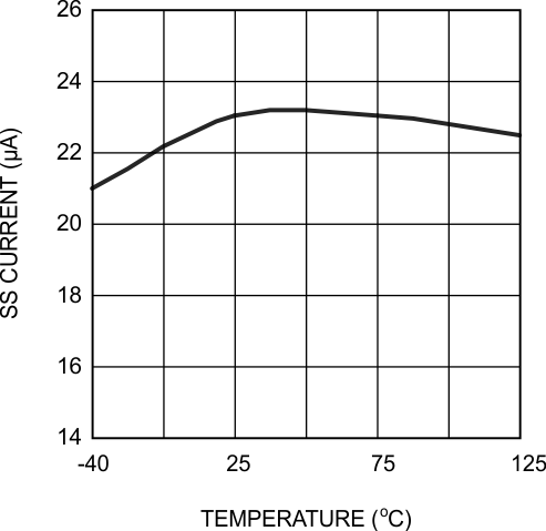
| Soft-start current source normal | TJ = 25°C | 22 | µA | ||||
| over full operating junction temperature | 17 | 27 | |||||
| Soft-start current source following a CS2 event | TJ = 25°C | 1 | µA | ||||
| over full operating junction temperature | 0.5 | 1.5 | |||||
| OSCILLATOR | |||||||
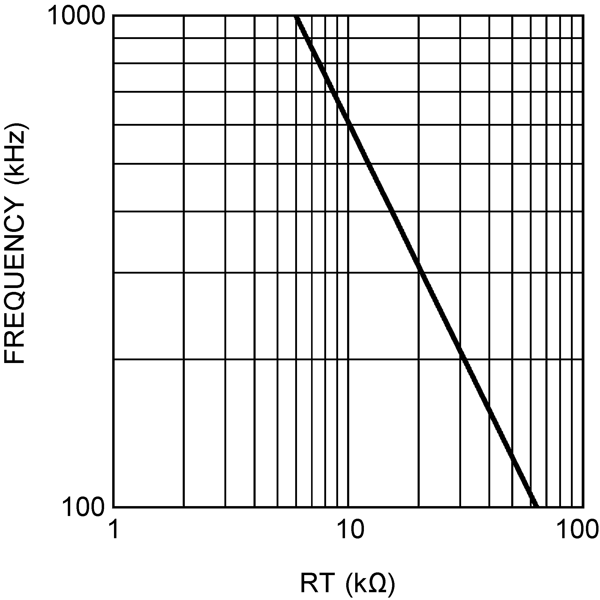
| Frequency1 | TA = 25°C, | 180 | 200 | 220 | kHz | ||
| TJ = Tlow to Thigh | 175 | 225 | |||||
| Frequency2 | RT = 10.4 kΩ | TA = 25°C, | 580 | kHz | |||
| TJ = Tlow to Thigh | 510 | 650 | |||||
| Sync threshold | 2 | V | |||||
| Min sync pulse width | TJ = Tlow to Thigh | 100 | ns | ||||
| Sync frequency range | TJ = Tlow to Thigh | 160 | kHz | ||||
| PWM COMPARATOR | |||||||
| Delay to output | COMP step 5 V to 0 V, Time to onset of OUT_A transition low |
40 | ns | ||||
| Duty cycle range | TJ = Tlow to Thigh | 0% | 80% | ||||
| COMP to PWM offset | TA = 25°C, | 1 | V | ||||
| TJ = Tlow to Thigh | 0.7 | 1.3 | |||||
| COMP open-circuit voltage | TJ = Tlow to Thigh | 4.3 | 5.9 | V | |||
| COMP short-circuit current | COMP = 0 V | TA = 25°C, | 1 | mA | |||
| TJ = Tlow to Thigh | 0.6 | 1.4 | |||||
| VOLT × SECOND CLAMP | |||||||
| Ramp clamp level | Delta RAMP measured from onset of OUT_A to Ramp peak, COMP = 5 V |
TA = 25°C, | 2.5 | V | |||
| TJ = Tlow to Thigh | 2.4 | 2.6 | |||||
| UVLO SHUTDOWN | |||||||
| Undervoltage shutdown threshold | TA = 25°C, | 2.5 | V | ||||
| TJ = Tlow to Thigh | 2.44 | 2.56 | |||||
| Undervoltage shutdown hysteresis | TA = 25°C, | 20 | µA | ||||
| TJ = Tlow to Thigh | 16 | 24 | |||||
| OUTPUT SECTION | |||||||
| OUT_A high saturation | MOS device at Iout = –10 mA |
TA = 25°C, | 5 | Ω | |||
| TJ = Tlow to Thigh | 10 | ||||||
| OUTPUT_A peak current sink | Bipolar Device at Vcc/2 | 3 | A | ||||
| OUT_A low saturation | MOS device at Iout = 10 mA |
TA = 25°C, | 6 | Ω | |||
| TJ = Tlow to Thigh | 9 | ||||||
| OUTPUT_A rise time | Cgate = 2.2 nF | 20 | ns | ||||
| OUTPUT_A fall time | Cgate = 2.2 nF | 15 | ns | ||||
| OUT_B high saturation | MOS device at Iout = –10 mA |
TA = 25°C, | 10 | Ω | |||
| TJ = Tlow to Thigh | 20 | ||||||
| OUTPUT_B peak current sink | Bipolar device at Vcc/2 | 1 | A | ||||
| OUT_B low saturation | MOS device at Iout = 10 mA |
TA = 25°C, | 12 | Ω | |||
| TJ = Tlow to Thigh | 18 | ||||||
| OUTPUT_B rise time | Cgate = 1 nF | 20 | ns | ||||
| OUTPUT_B fall time | Cgate = 1 nF | 15 | ns | ||||
| OUTPUT TIMING CONTROL | |||||||
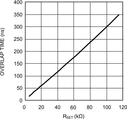
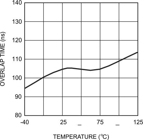
| Overlap time | RSET = 38 kΩ connected to GND, 50% to 50% transitions |
TA = 25°C, | 105 | ns | |||
| TJ = Tlow to Thigh | 75 | 135 | |||||
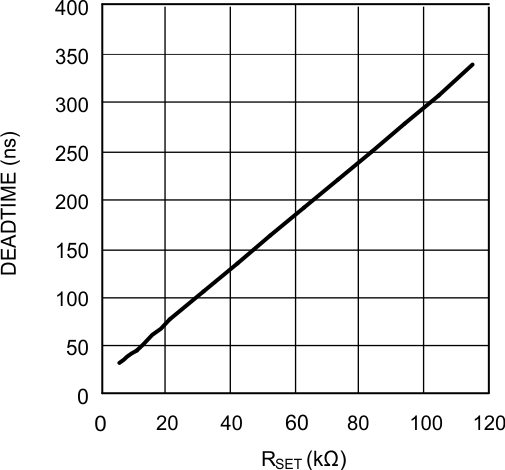
| Dead time | RSET = 29.5 kΩ connected to REF, 50% to 50% transitions |
TA = 25°C, | 105 | ns | |||
| TJ = Tlow to Thigh | 75 | 135 | |||||
| THERMAL SHUTDOWN | |||||||
| TSD | Thermal shutdown threshold | 165 | °C | ||||
| Thermal shutdown hysteresis | 25 | °C | |||||
(1) All electrical characteristics having room temperature limits are tested during production with TA = TJ = 25°C. All hot and cold limits are specified by correlating the electrical characteristics to process and temperature variations and applying statistical process control.
(2) Device thermal limitations may limit usable range.
6.6 Typical Characteristics
| RSET = 38 K |
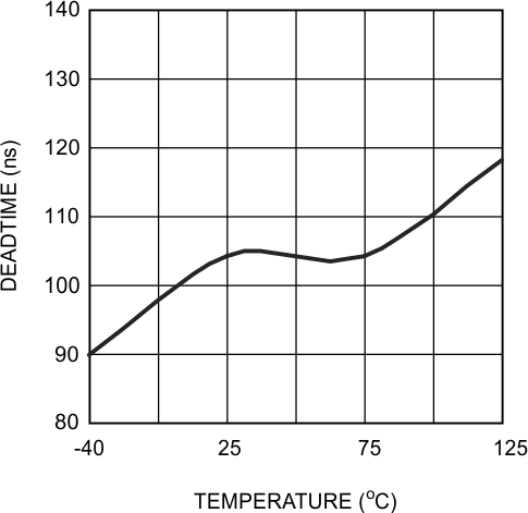
| RSET = 29.5 K |