SNVS265C December 2003 – January 2016 LM5025
PRODUCTION DATA.
- 1 Features
- 2 Applications
- 3 Description
- 4 Revision History
- 5 Pin Configuration and Functions
- 6 Specifications
- 7 Detailed Description
- 8 Application and Implementation
- 9 Power Supply Recommendations
- 10Layout
- 11Device and Documentation Support
- 12Mechanical, Packaging, and Orderable Information
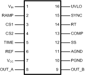
5 Pin Configuration and Functions
PW and NHQ Packages
16-Pin TSSOP and WSON
Top View

Pin Functions
| PIN | I/O(1) | DESCRIPTION | APPLICATION INFORMATION | |
|---|---|---|---|---|
| NO. | NAME | |||
| 1 | VIN | I | Source input voltage | Input to start-up regulator. Input 13 V to 90 V, with transient capability to 100 V. |
| 2 | RAMP | I | Modulator ramp signal | An external RC circuit from Vin sets the ramp slope. This pin is discharged at the conclusion of every cycle by an internal FET, initiated by either the internal clock or the V*Sec Clamp comparator. |
| 3 | CS1 | I | Current sense input for cycle-by-cycle limiting | If CS1 exceeds 0.25 V the outputs goes into Cycle-by-Cycle current limit. CS1 is held low for 50 ns after OUT_A switches high providing leading edge blanking. |
| 4 | CS2 | I | Current sense input for soft restart | If CS2 exceeds 0.25 V the outputs are disabled and a soft-start commences. The soft-start capacitor is fully discharged and then released with a pullup current of 1 µA. After the first output pulse (when SS = 1 V), the SS charge current reverts back to 20 µA. CS2 is held low for 50 ns after OUT_A switches high, providing leading edge blanking. |
| 5 | TIME | I | Output overlap and deadtime control | An external resistor (RSET) sets either the overlap time or dead time for the active clamp output. An RSET resistor connected between TIME and GND produces in-phase OUT_A and OUT_B pulses with overlap. An RSET resistor connected between TIME and REF produces out-of-phase OUT_A and OUT_B pulses with deadtime. |
| 6 | REF | O | Precision 5-V reference output | Maximum output current: 10-mA locally decouple with a 0.1-µF capacitor. Reference stays low until the line UVLO and the VCC UV comparators are satisfied. |
| 7 | VCC | P | Output from the internal high-voltage start-up regulator. The VCC voltage is regulated to 7.6 V | If an auxiliary winding raises the voltage on this pin above the regulation setpoint, the internal start-up regulator shutdowns, reducing the IC power dissipation. |
| 8 | OUT_A | O | Main output driver | Output of the main switch PWM output gate driver. Output capability of 3-A peak sink current. |
| 9 | OUT_B | O | Active clamp output driver | Output of the active clamp switch gate driver. Capable of 1.25-A peak sink current.. |
| 10 | PGND | G | Power ground | Connect directly to analog ground. |
| 11 | AGND | G | Analog ground | Connect directly to power ground. For the WSON package option the exposed pad is electrically connected to AGND. |
| 12 | SS | I | Soft-start control | An external capacitor and an internal 20-µA current source set the soft-start ramp. The SS current source is reduced to 1 µA initially following a CS2 overcurrent event or an over temperature event. |
| 13 | COMP | I | Input to the pulse width modulator | An internal 5-KΩ resistor pullup is provided on this pin. The external opto-coupler sinks current from COMP to control the PWM duty cycle. |
| 14 | RT | I | Oscillator timing resistor pin | An external resistor connected from RT to ground sets the internal oscillator frequency. |
| 15 | SYNC | I | Oscillator UP and DOWN synchronization input | The internal oscillator can be synchronized to an external clock with a frequency 20% lower than the internal oscillator’s free running frequency. There is no constraint on the maximum sync frequency. |
| 16 | UVLO | I | Line undervoltage shutdown | An external voltage divider from the power source sets the shutdown comparator levels. The comparator threshold is 2.5 V. Hysteresis is set by an internal current source (20 µA) that is switched on or off as the UVLO pin potential crosses the 2.5-V threshold. |
(1) P = power, G = ground, I = input, O = Output, I/O = Input/output