SNVS265C December   2003  – January 2016 LM5025

PRODUCTION DATA.  

  1. Features
  2. Applications
  3. Description
  4. Revision History
  5. Pin Configuration and Functions
  6. Specifications
    1. 6.1 Absolute Maximum Ratings
    2. 6.2 ESD Ratings
    3. 6.3 Recommended Operating Conditions
    4. 6.4 Thermal Information
    5. 6.5 Electrical Characteristics
    6. 6.6 Typical Characteristics
  7. Detailed Description
    1. 7.1 Overview
    2. 7.2 Functional Block Diagram
    3. 7.3 Feature Description
      1. 7.3.1  High-Voltage Start-Up Regulator
      2. 7.3.2  Line Undervoltage Detector
      3. 7.3.3  PWM Outputs
      4. 7.3.4  Compound Gate Drivers
      5. 7.3.5  PWM Comparator
      6. 7.3.6  Volt Second Clamp
      7. 7.3.7  Current Limit
      8. 7.3.8  Oscillator and Sync Capability
      9. 7.3.9  Feed-Forward Ramp
      10. 7.3.10 Soft-Start
      11. 7.3.11 Thermal Protection
    4. 7.4 Device Functional Modes
  8. Application and Implementation
    1. 8.1 Application Information
    2. 8.2 Typical Application
      1. 8.2.1 Design Requirements
      2. 8.2.2 Detailed Design Procedure
        1. 8.2.2.1 Oscillator
        2. 8.2.2.2 Soft-Start Ramp Time and Hiccup Interval
        3. 8.2.2.3 Feed-Forward Ramp and Maximum On Time Clamp
        4. 8.2.2.4 Dead Times
      3. 8.2.3 Application Curves
      4. 8.2.4 System Example
  9. Power Supply Recommendations
  10. 10Layout
    1. 10.1 Layout Guidelines
    2. 10.2 Layout Example
  11. 11Device and Documentation Support
    1. 11.1 Documentation Support
      1. 11.1.1 Related Documentation
    2. 11.2 Community Resources
    3. 11.3 Trademarks
    4. 11.4 Electrostatic Discharge Caution
    5. 11.5 Glossary
  12. 12Mechanical, Packaging, and Orderable Information

封装选项

机械数据 (封装 | 引脚)
散热焊盘机械数据 (封装 | 引脚)
订购信息

10 Layout

10.1 Layout Guidelines

  • Connect two grounds PGND (power ground) and AGND (analog ground) directly as device ground ICGND. The connection must be as close to the pins as possible.
  • If there are multiple PCB layers and there is a inner ground layer, use two vias or one big via on GND and connect them to the inner ground layer (ICGND).
  • The power stage ground PSGND should be separated with the ICGND. PSGND and ICGND should be connected at a single point close to the device.
  • The bypass capacitors to the VCC pin and REF pin should be as close as possible to the pins and ground (ICGND).
  • The filtering capacitors connected to CS1 and CS2 pins should have connections as short as possible to ICGND; if an inner ground layer is available, use vias to connect the capacitors to the ground layer (ICGND).
  • The resistors and capacitors connected to the timing configuration pins should be as close as possible to the pins and ground (ICGND).

10.2 Layout Example
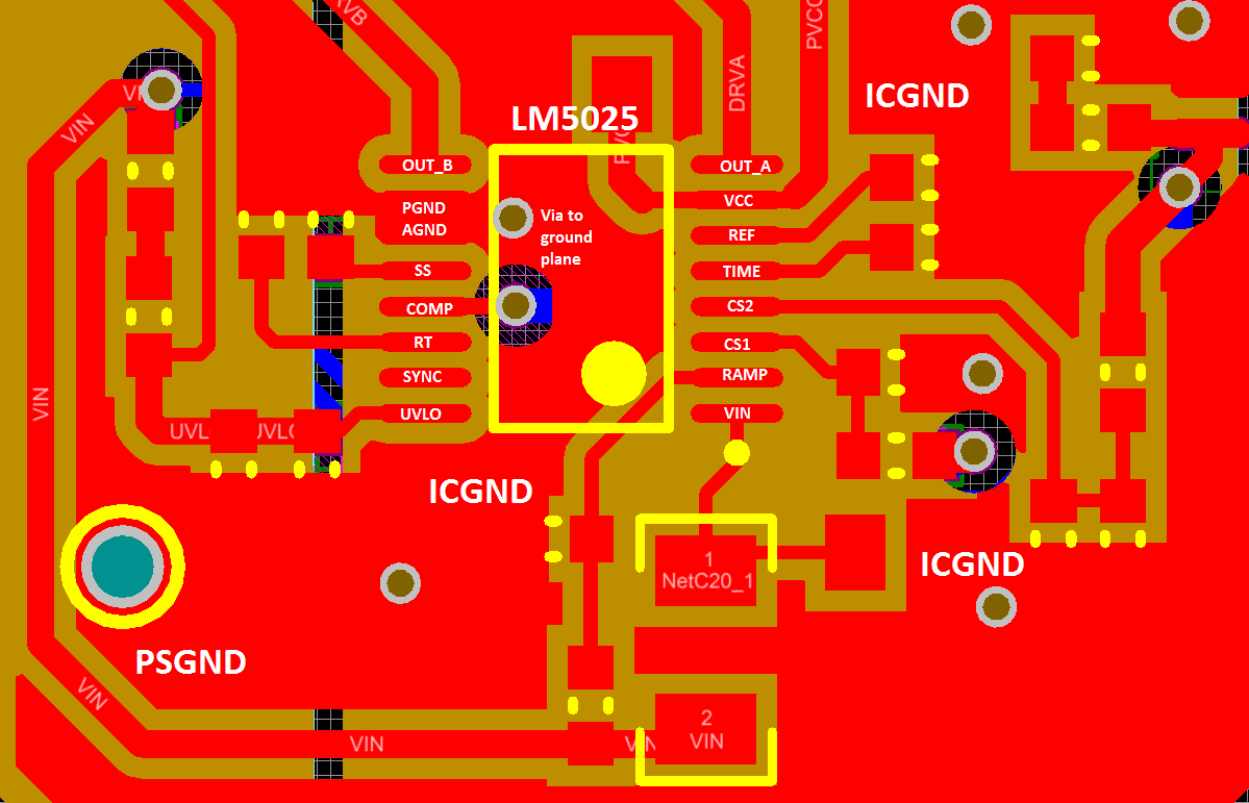
LM5025 Layout Example.gif Figure 22. LM5025 Layout Recommendation