SNAS470E October 2008 – November 2015 LM48100Q-Q1
PRODUCTION DATA.
- 1 Features
- 2 Applications
- 3 Description
- 4 Revision History
- 5 Pin Configuration and Functions
-
6 Specifications
- 6.1 Absolute Maximum Ratings
- 6.2 ESD Ratings
- 6.3 Recommended Operating Conditions
- 6.4 Thermal Information
- 6.5 Electrical Characteristics for VDD = 5 V
- 6.6 Electrical Characteristics for VDD = 5 V at Extended Temperature Limits
- 6.7 Electrical Characteristics for VDD = 3.6 V
- 6.8 Electrical Characteristics for VDD = 3.6 V at Extended Temperature Limits
- 6.9 I2C Interface Characteristics for VDD = 5 V, 2.2 V ≤ I2C VDD ≤ 5.5 V
- 6.10 I2C Interface Characteristics for VDD = 5 V, 1.8 V ≤ I2C VDD ≤ 2.2 V
- 6.11 Typical Characteristics
-
7 Detailed Description
- 7.1 Overview
- 7.2 Functional Block Diagram
- 7.3 Feature Description
- 7.4 Device Functional Modes
- 7.5 Programming
- 7.6 Register Maps
- 8 Application and Implementation
- 9 Power Supply Recommendations
- 10Layout
- 11Device and Documentation Support
- 12Mechanical, Packaging, and Orderable Information
1 Features
- Output Fault Detection
- I2C Volume and Mode Control
- Input Mixer and Multiplexer
- High PSRR
- Individual 32-Step Volume Control
- Short Circuit and Thermal Protection
- Advanced Click-and-Pop Suppression
- Low-Power Shutdown Mode
- Available in 14-Pin HTSSOP Package
- Key Specifications:
- Output Power at VDD = 5 V, RL = 8 Ω,
THD+N ≤ 1% 1.3 W (Typical) - Quiescent Power Supply Current at 5 V,
6 mA (Typical) - PSRR at 1 kHz 74 dB (Typical)
- Shutdown current 0.01 μA (Typical)
- Output Power at VDD = 5 V, RL = 8 Ω,
2 Applications
- Automotive Instrument Clusters
- Hands-Free Car Kits
- Medical
3 Description
The LM48100Q-Q1 is a single supply, mono, bridge-tied load amplifier with I2C volume control, ideal for automotive applications. A comprehensive output fault detection system senses the load conditions, protecting the device during short circuit events, as well as detecting open circuit conditions.
Operating from a single 5-V supply, the LM48100Q-Q1 delivers 1.3 W of continuous output power to an 8 Ω load with < 1% THD+N. Flexible power supply requirements allow operation from 3 V to 5.5 V. High power supply rejection ratio (PSRR), 74 dB at 1 kHz, allows the device to operate in noisy environments without additional power supply conditioning.
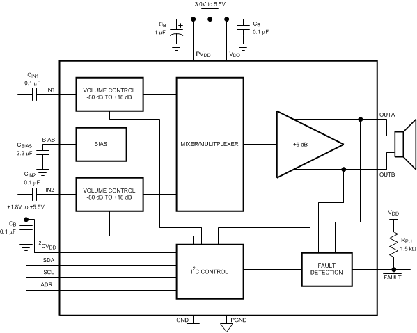
The LM48100Q-Q1 features dual audio inputs that can be mixed/multiplexed to the device output. Each input path has its own independent, 32-step volume control. The mixer, volume control and device mode select are controlled through an I2C compatible interface. An open drain FAULT output indicates when a fault has occurred. Comprehensive output short circuit and thermal overload protection prevent the device from being damaged during a fault condition.
A low power shutdown mode reduces supply current consumption to 0.01 µA. Superior click and pop suppression eliminates audible transients on power-up/down and during shutdown. The LM48100Q-Q1 is available in an 14-pin HTSSOP PowerPAD™ IC package.
Device Information(1)
| PART NUMBER | PACKAGE | BODY SIZE (NOM) |
|---|---|---|
| LM48100Q-Q1 | HTSSOP (14) | 5.00 mm × 4.40 mm |
- For all available packages, see the orderable addendum at the end of the datasheet.
Typical Audio Amplifier Application Circuit
