ZHCSGJ7A July   2017  – October 2017 LM36011

PRODUCTION DATA.  

  1. 特性
  2. 应用
  3. 说明
  4. 修订历史记录
  5. Pin Configuration and Functions
  6. Specifications
    1. 6.1 Absolute Maximum Ratings
    2. 6.2 ESD Ratings
    3. 6.3 Recommended Operating Conditions
    4. 6.4 Thermal Information
    5. 6.5 Electrical Characteristics
    6. 6.6 Timing Requirements
    7. 6.7 Typical Characteristics
  7. Detailed Description
    1. 7.1 Overview
    2. 7.2 Functional Block Diagram
    3. 7.3 Feature Description
      1. 7.3.1 Flash Mode
      2. 7.3.2 Torch Mode
      3. 7.3.3 IR Mode
    4. 7.4 Device Functioning Modes
      1. 7.4.1 Start-Up (Enabling The Device)
      2. 7.4.2 Input Voltage Flash Monitor (IVFM)
      3. 7.4.3 Fault/Protections
        1. 7.4.3.1 Input Voltage Flash Monitor (IVFM)
        2. 7.4.3.2 LED Short Fault
        3. 7.4.3.3 Thermal Scale-Back (TSB)
        4. 7.4.3.4 Thermal Shutdown (TSD)
        5. 7.4.3.5 Undervoltage Lockout (UVLO)
        6. 7.4.3.6 Flash Time-out (FTO)
    5. 7.5 Programming
      1. 7.5.1 Control Truth Table
      2. 7.5.2 I2C-Compatible Interface
        1. 7.5.2.1 Data Validity
        2. 7.5.2.2 Start and Stop Conditions
        3. 7.5.2.3 Transferring Data
        4. 7.5.2.4 I2C-Compatible Chip Address
    6. 7.6 Register Descriptions
      1. 7.6.1 Enable Register (0x01)
      2. 7.6.2 Configuration Register (0x02)
      3. 7.6.3 LED Flash Brightness Register (0x03)
      4. 7.6.4 LED Torch Brightness Register (0x04)
      5. 7.6.5 Flags Register (0x05)
      6. 7.6.6 Device ID and RESET Register (0x06)
  8. Applications and Implementation
    1. 8.1 Application Information
    2. 8.2 Typical Application
      1. 8.2.1 Design Requirements
      2. 8.2.2 Detailed Design Procedure
        1. 8.2.2.1 Thermal Performance
        2. 8.2.2.2 Input Capacitor Selection
      3. 8.2.3 Application Curves
  9. Power Supply Recommendations
  10. 10Layout
    1. 10.1 Layout Guidelines
    2. 10.2 Layout Example
  11. 11器件和文档支持
    1. 11.1 器件支持
      1. 11.1.1 Third-Party Products Disclaimer
    2. 11.2 文档支持
      1. 11.2.1 相关文档
    3. 11.3 商标
    4. 11.4 静电放电警告
    5. 11.5 Glossary
  12. 12机械、封装和可订购信息

封装选项

机械数据 (封装 | 引脚)
散热焊盘机械数据 (封装 | 引脚)
订购信息

Layout

Layout Guidelines

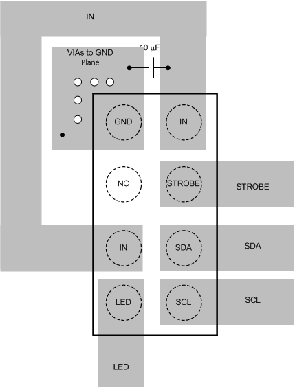
The following steps are to be used as a reference to ensure the device is stable and maintains proper LED current regulation across its intended operating voltage and current range.

  1. Place CIN on the top layer (same layer as the LM36011) and as close as possible to the device. Connecting the input capacitor through short, wide traces to both the IN and GND pins reduces the inductive voltage spikes that occur during switching which can corrupt the VIN line.
  2. Terminate the flash LED cathode directly to the GND pin of the LM36011. If possible, route the LED return with a dedicated path so as to keep the high amplitude LED current out of the GND plane. For a flash LED that is routed relatively far away from the LM36011, a good approach is to sandwich the forward and return current paths over the top of each other on two layers. This helps reduce the inductance of the LED current path.

Layout Example

LM36011 LM36011_Layout_Example.gif Figure 45. LM36011 Layout Example