ZHCSGJ8B April   2017  – October 2017 LM36010

PRODUCTION DATA.  

  1. 特性
  2. 应用
  3. 说明
    1.     Device Images
      1.      简化电路原理图
  4. 修订历史记录
  5. Pin Configuration and Functions
    1.     Pin Functions
  6. Specifications
    1. 6.1 Absolute Maximum Ratings
    2. 6.2 ESD Ratings
    3. 6.3 Recommended Operating Conditions
    4. 6.4 Thermal Information
    5. 6.5 Electrical Characteristics
    6. 6.6 Timing Requirements
    7. 6.7 Switching Characteristics
    8. 6.8 Typical Characteristics
  7. Detailed Description
    1. 7.1 Overview
    2. 7.2 Functional Block Diagram
    3. 7.3 Feature Description
      1. 7.3.1 Flash Mode
      2. 7.3.2 Torch Mode
      3. 7.3.3 IR Mode
    4. 7.4 Device Functioning Modes
      1. 7.4.1 Start-Up (Enabling The Device)
      2. 7.4.2 Pass Mode
      3. 7.4.3 Input Voltage Flash Monitor (IVFM)
      4. 7.4.4 Fault/Protections
        1. 7.4.4.1 Overvoltage Protection (OVP)
        2. 7.4.4.2 Input Voltage Flash Monitor (IVFM)
        3. 7.4.4.3 LED and/or VOUT Short Fault
        4. 7.4.4.4 Current Limit (OCP)
        5. 7.4.4.5 Thermal Scale-Back (TSB)
        6. 7.4.4.6 Thermal Shutdown (TSD)
        7. 7.4.4.7 Undervoltage Lockout (UVLO)
        8. 7.4.4.8 Flash Time-out (FTO)
    5. 7.5 Programming
      1. 7.5.1 Control Truth Table
      2. 7.5.2 I2C-Compatible Interface
        1. 7.5.2.1 Data Validity
        2. 7.5.2.2 Start and Stop Conditions
        3. 7.5.2.3 Transferring Data
        4. 7.5.2.4 I2C-Compatible Chip Address
    6. 7.6 Register Descriptions
      1. 7.6.1 Enable Register (0x01)
      2. 7.6.2 Configuration Register (0x02)
      3. 7.6.3 LED Flash Brightness Register (0x03)
      4. 7.6.4 LED Torch Brightness Register (0x04)
      5. 7.6.5 Flags Register (0x05)
      6. 7.6.6 Device ID and RESET Register (0x06)
  8. Applications and Implementation
    1. 8.1 Application Information
    2. 8.2 Typical Application
      1. 8.2.1 Design Requirements
      2. 8.2.2 Detailed Design Procedure
        1. 8.2.2.1 Thermal Performance
        2. 8.2.2.2 Output Capacitor Selection
        3. 8.2.2.3 Input Capacitor Selection
        4. 8.2.2.4 Inductor Selection
      3. 8.2.3 Application Curves
  9. Power Supply Recommendations
  10. 10Layout
    1. 10.1 Layout Guidelines
    2. 10.2 Layout Example
  11. 11器件和文档支持
    1. 11.1 器件支持
      1. 11.1.1 Third-Party Products Disclaimer
    2. 11.2 文档支持
      1. 11.2.1 相关文档
    3. 11.3 接收文档更新通知
    4. 11.4 社区资源
    5. 11.5 商标
    6. 11.6 静电放电警告
    7. 11.7 Glossary
  12. 12机械、封装和可订购信息

封装选项

请参考 PDF 数据表获取器件具体的封装图。

机械数据 (封装 | 引脚)
  • YKB|8
散热焊盘机械数据 (封装 | 引脚)
订购信息

IR Mode

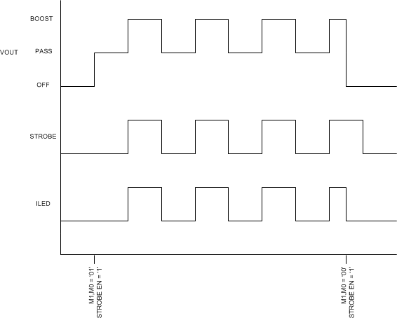
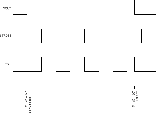
In IR mode, the target LED current is equal to the value stored in the LED Flash Brightness Register (0x03 bits [7:0]). When IR mode is enabled by the Enable Register (0x01) setting mode M1, M0 (bits [1:0]) to 01, the boost converter turns on and sets the output equal to the input (pass mode). In IR mode, toggling the STROBE pin enables and disables the LED current source. The STROBE pin can only be set to be Level sensitive, as all timing of the IR pulse is externally controlled. In IR mode, the current source does not control the ramp rate of the LED output. The current transitions immediately from off to on and then on to off.
LM36010 IRBOOST.gif
If needed, the DC/DC boost will turn on when the LED current is delivered (Strobe Pin = High). When the Strobe Pin goes low, the output voltage will return to VIN (Pass Mode)
Figure 29. IR Mode with Boost
LM36010 IRPASS.gif
In pass mode, the boost stays disabled and VOUT = VIN when the Strobe Pin is high or low
Figure 30. IR Mode Pass Only
LM36010 TIMEOUTIR.gif
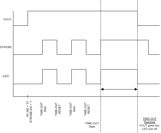
When the flash timer elapses, the device goes into stand-by regardless of strobe state
Figure 31. IR Mode Time-out