ZHCSGW9 October 2017 LM2623-Q1
PRODUCTION DATA.
10 Layout
10.1 Layout Guidelines
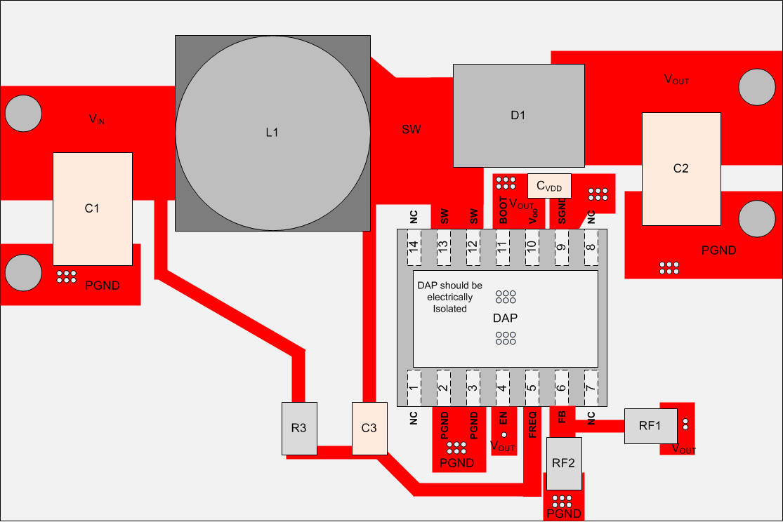
Figure 12 follows proper layout guidelines — use as a guide for laying out the LM2623-Q1 circuit. The LM2623-Q1 inductive boost converter sees a high switched voltage at the SW pin and a step current through the Schottky diode and output capacitor each switching cycle. The high switching voltage can create interference into nearby nodes due to electric field coupling (I = C × dV/dt). The large step current through the diode and the output capacitor can cause a large voltage spike at the SW and BOOST pins due to parasitic inductance in the step current conducting path (V = L × di/dt). Board layout guidelines are geared towards minimizing this electric field coupling and conducted noise.
Boost Output Capacitor Placement, Schottky Diode Placement, and Boost Input / VDD Capacitor Placement detail the main (layout sensitive) areas of the LM2623-Q1 inductive boost converter in order of decreasing importance:
10.1.1 Boost Output Capacitor Placement
Because the output capacitor is in the path of the inductor current discharge path, it experiences a high-current step from 0 A to the peak inductor current each time the switch turns off, and the Schottky diode turns on. Any inductance along this series path from the diodes cathode, through COUT, and back into the LM2623-Q1 GND pin contributes to voltage spikes at SW. These spikes can potentially overvoltage the SW and BOOST pins, or feed through to GND. To avoid this, COUT+ must be connected as close as possible to the cathode of the Schottky diode, and COUT− must be connected as close as possible to the LM2623-Q1 GND bumps. The best placement for COUT is on the same layer as the LM2623-Q1 to avoid any vias that can add excessive series inductance.
10.1.2 Schottky Diode Placement
In the LM2623-Q1 device boost circuit the Schottky diode is in the path of the inductor current discharge. As a result the Schottky diode detects a high-current step from 0 A to the peak inductor current each time the switch turns off, and the diode turns on. Any inductance in series with the diode causes a voltage spike at SW. This can potentially overvoltage the SW pin, or feed through to VOUT and through the output capacitor, into GND. Connecting the anode of the diode as close as possible to the SW pin, and connecting the cathode of the diode as close as possible to COUT reduces the parasitic inductance and minimizes these voltage spikes.
10.1.3 Boost Input / VDD Capacitor Placement
The LM2623-Q1 input capacitor filters the inductor current ripple and the internal MOSFET driver currents. The inductor current ripple can add input voltage ripple due to any series resistance in the input power path. The MOSFET driver currents can add voltage spikes on the input due to the inductance in series with the VIN/VDD and the input capacitor. Place the input capacitor close to the inductor and minimize the current-loop area. Close placement of the VDD capacitor to the VDD and GND pins is critical because any series inductance can create voltage spikes that could appear on the VIN/VDD supply line.
10.2 Layout Example
 Figure 12. LM2623-Q1 Layout Example
10.3 WSON Package Devices
The LM2623-Q1 is offered in the 14-pin WSON surface mount package — for details of the thermal performance as well as mounting and soldering specifications, refer to Leadless Leadframe Package (LLP).