SNVS771C May 1998 – December 2016 LM138 , LM338
PRODUCTION DATA.
- 1 Features
- 2 Applications
- 3 Description
- 4 Revision History
- 5 Pin Configuration and Functions
- 6 Specifications
- 7 Detailed Description
- 8 Application and Implementation
- 9 Power Supply Recommendations
- 10Layout
- 11Device and Documentation Support
- 12Mechanical, Packaging, and Orderable Information
6 Specifications
6.1 Absolute Maximum Ratings
over operating free-air temperature range (unless otherwise noted)(1)| MIN | MAX | UNIT | ||
|---|---|---|---|---|
| Input and output voltage differential | –0.3 | 40 | V | |
| Power dissipation | Internally limited | |||
| Lead temperature | TO-3 package (soldering, 10 s) | 300 | °C | |
| TO-220 package (soldering, 4 s) | 260 | |||
| Operating temperature, TJ | LM138 | –55 | 150 | °C |
| LM338 | 0 | 125 | ||
| Storage temperature, Tstg | –65 | 150 | °C | |
(1) Stresses beyond those listed under Absolute Maximum Ratings may cause permanent damage to the device. These are stress ratings only, which do not imply functional operation of the device at these or any other conditions beyond those indicated under Recommended Operating Conditions. Exposure to absolute-maximum-rated conditions for extended periods may affect device reliability.
6.2 Recommended Operating Conditions
over operating free-air temperature range (unless otherwise noted)| MIN | MAX | UNIT | |
|---|---|---|---|
| Input-to-output voltage differential | 3 | 40 | V |
| Output current | 5 | A |
6.3 Thermal Information
| THERMAL METRIC(1) | LM338 | LM338 | UNIT | ||
|---|---|---|---|---|---|
| NDS (TO-CAN) | NDE (TO-220) | NDS (TO-CAN) | |||
| 2 PINS | 3 PINS | 2 PINS | |||
| RθJA | Junction-to-ambient thermal resistance | 35 | 22.9 | 35 | °C/W |
| RθJC(top) | Junction-to-case (top) thermal resistance | 1 | 15.7 | 1 | °C/W |
| RθJB | Junction-to-board thermal resistance | — | 4.1 | — | °C/W |
| ψJT | Junction-to-top characterization parameter | — | 2.1 | — | °C/W |
| ψJB | Junction-to-board characterization parameter | — | 4.1 | — | °C/W |
| RθJC(bot) | Junction-to-case (bottom) thermal resistance | — | 0.7 | — | °C/W |
(1) For more information about traditional and new thermal metrics, see the Semiconductor and IC Package Thermal Metrics application report.
6.4 Electrical Characteristics: LM138
Values apply for TJ = 25°C; VIN – VOUT = 5 V; and IOUT = 10 mA (unless otherwise noted).(1)| PARAMETER | TEST CONDITIONS | MIN | TYP | MAX | UNIT | ||
|---|---|---|---|---|---|---|---|
| VREF | Reference voltage | 3 V ≤ (VIN – VOUT) ≤ 35 V, 10 mA ≤ IOUT ≤ 5 A, P ≤ 50 W, TJ = –55°C to 150°C |
1.19 | 1.24 | 1.29 | V | |
| VRLINE | Line regulation | 3 V ≤ (VIN – VOUT) ≤ 35 V(2) | TJ = 25°C | 0.005% | 0.01% | V | |
| TJ = –55°C to 150°C | 0.02% | 0.04% | V | ||||
| VRLOAD | Load regulation | 10 mA ≤ IOUT ≤ 5 A(2) | TJ = 25°C | 0.1% | 0.3% | ||
| TJ = –55°C to 150°C | 0.3% | 0.6% | |||||
| Thermal regulation | 20 ms pulse | 0.002% | 0.01% | W | |||
| IADJ | Adjustment pin current | TJ = –55°C to 150°C | 45 | 100 | µA | ||
| ΔIADJ | Adjustment pin current change | 10 mA ≤ IOUT ≤ 5 A, 3 V ≤ (VIN – VOUT) ≤ 35 V, TJ = –55°C to 150°C |
0.2 | 5 | µA | ||
| ΔVR/T | Temperature stability | TJ = –55°C to 150°C | 1% | ||||
| ILOAD(MIN) | Minimum load current | VIN – VOUT = 35 V, TJ = –55°C to 150°C | 3.5 | 5 | mA | ||
| ICL | Current limit | VIN – VOUT ≤ 10 V | |||||
| DC, TJ = –55°C to 150°C | 5 | 8 | A | ||||
| 0.5-ms peak, TJ = –55°C to 150°C | 7 | 12 | A | ||||
| VIN – VOUT = 30 V | 1 | 1 | A | ||||
| VN | RMS output noise (percent of VOUT) |
10 Hz ≤ f ≤ 10 kHz | 0.003% | ||||
| ΔVR/ΔVIN | Ripple rejection ratio | VOUT = 10 V, f = 120 Hz, CADJ = 0 µF, TJ = –55°C to 150°C |
60 | dB | |||
| VOUT = 10 V, f = 120 Hz, CADJ = 10 µF, TJ = –55°C to 150°C |
60 | 75 | dB | ||||
| Long-term stability | TJ = 125°C, 1000 Hrs | 0.3% | 1% | ||||
(1) These specifications are applicable for power dissipations up to 50 W for the TO-3 (NDS) package and 25 W for the TO-220 (NDE) package. Power dissipation is specified at these values up to 15-V input-output differential. Above 15-V differential, power dissipation is limited by internal protection circuitry. All limits (that is, the numbers in the minimum and maximum columns) are specified to TI's AOQL (Average Outgoing Quality Level).
(2) Regulation is measured at a constant junction temperature, using pulse testing with a low duty cycle. Changes in output voltage due to heating effects are covered under the specifications for thermal regulation.
6.5 Electrical Characteristics: LM338
Values apply for TJ = 25°C; VIN – VOUT = 5 V; and IOUT = 10 mA (unless otherwise noted).(1)| PARAMETER | TEST CONDITIONS | MIN | TYP | MAX | UNIT | ||
|---|---|---|---|---|---|---|---|
| VREF | Reference voltage | 3 V ≤ (VIN – VOUT) ≤ 35 V, 10 mA ≤ IOUT ≤ 5 A, P ≤ 50 W, TJ = 0°C to 125°C |
1.19 | 1.24 | 1.29 | V | |
| VRLINE | Line regulation | 3 V ≤ (VIN – VOUT) ≤ 35 V(2) | TJ = 25°C | 0.005% | 0.03% | V | |
| TJ = 0°C to 125°C | 0.02% | 0.06% | V | ||||
| VRLOAD | Load regulation | 10 mA ≤ IOUT ≤ 5 A(2) | TJ = 25°C | 0.1 | 0.5 | ||
| TJ = 0°C to 125°C | 0.3 | 1 | |||||
| Thermal regulation | 20-ms pulse | 0.002% | 0.02% | W | |||
| IADJ | Adjustment pin current | TJ = 0°C to 125°C | 45 | 100 | µA | ||
| ΔIADJ | Adjustment pin current change | 10 mA ≤ IOUT ≤ 5 A, 3 V ≤ (VIN – VOUT) ≤ 35 V, TJ = 0°C to 125°C |
0.2 | 5 | µA | ||
| ΔVR/T | Temperature stability | TJ = 0°C to 125°C | 1 | ||||
| ILOAD(MIN) | Minimum load current | VIN – VOUT = 35 V, TJ = 0°C to 125°C | 3.5 | 10 | mA | ||
| ICL | Current limit | VIN – VOUT ≤ 10 V | |||||
| DC, TJ = 0°C to 125°C | 5 | 8 | A | ||||
| 0.5-ms peak, TJ = 0°C to 125°C | 7 | 12 | A | ||||
| VIN – VOUT = 30 V | 1 | A | |||||
| VN | RMS output noise (percent of VOUT) |
10 Hz ≤ f ≤ 10 kHz | 0.003% | ||||
| ΔVR/ΔVIN | Ripple rejection ratio | VOUT = 10 V, f = 120 Hz, CADJ = 0 µF, TJ = 0°C to 125°C |
60 | dB | |||
| VOUT = 10 V, f = 120 Hz, CADJ = 10 µF, TJ = 0°C to 125°C |
60 | 75 | dB | ||||
| Long-term stability | TJ = 125°C, 1000 Hrs | 0.3% | 1% | ||||
(1) These specifications are applicable for power dissipations up to 50 W for the TO-3 (NDS) package and 25 W for the TO-220 (NDE) package. Power dissipation is specified at these values up to 15-V input-output differential. Above 15-V differential, power dissipation is limited by internal protection circuitry. All limits (that is, the numbers in the minimum and maximum columns) are specified to TI's AOQL (Average Outgoing Quality Level).
(2) Regulation is measured at a constant junction temperature, using pulse testing with a low duty cycle. Changes in output voltage due to heating effects are covered under the specifications for thermal regulation.
6.6 Typical Characteristics
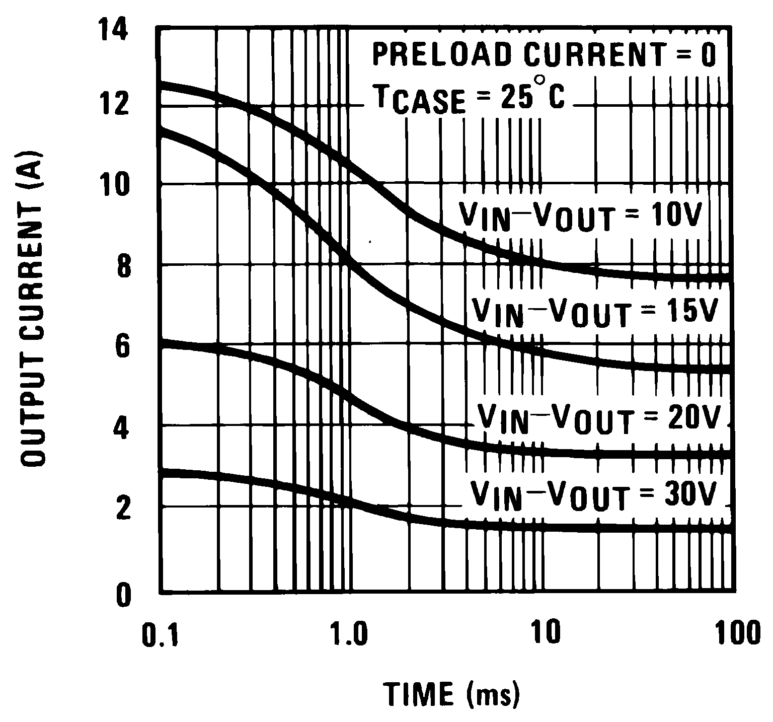 Figure 1. Current Limit
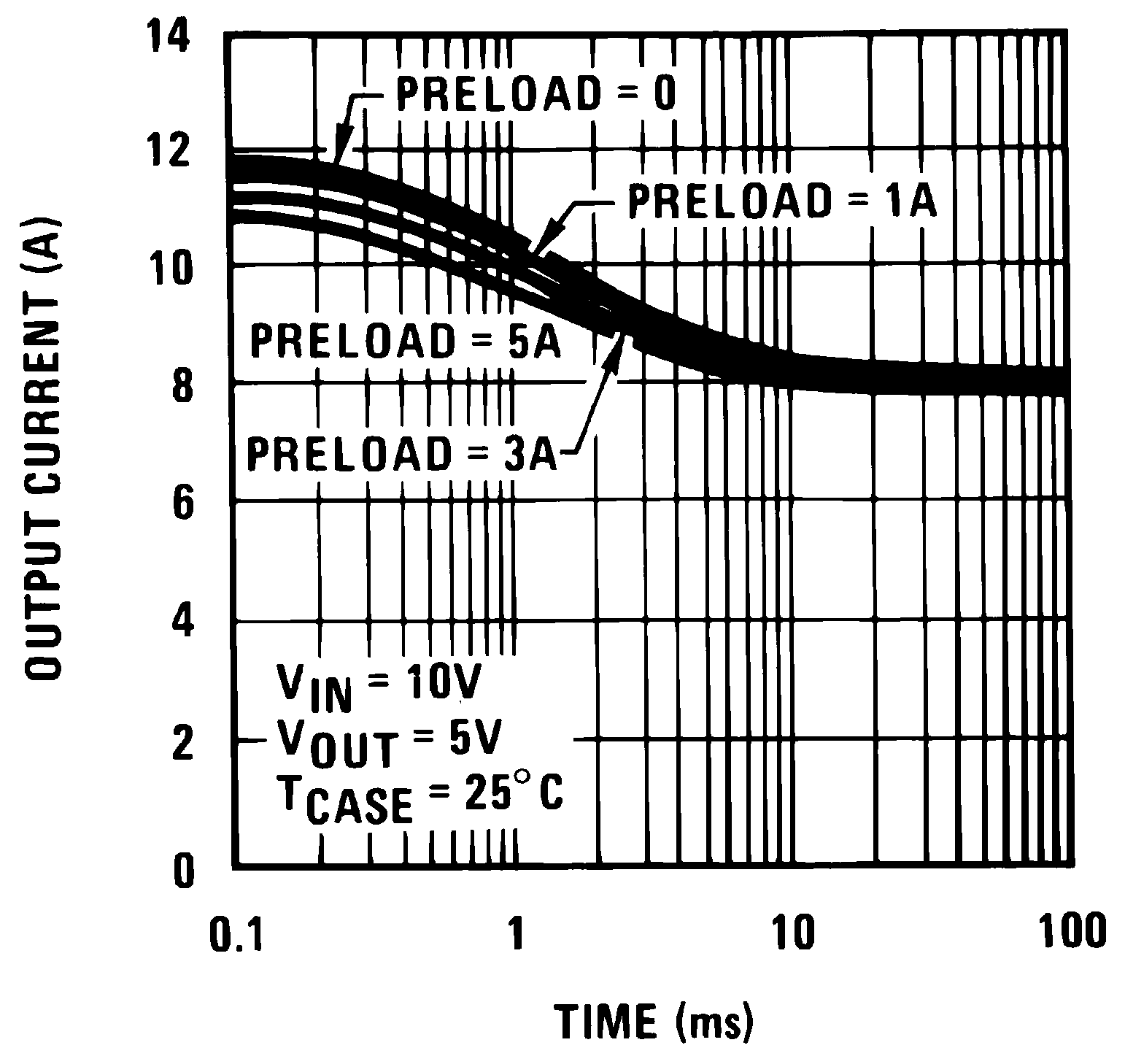 Figure 3. Current Limit
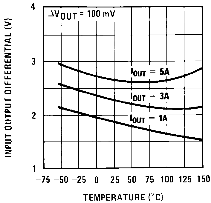 Figure 5. Dropout Voltage
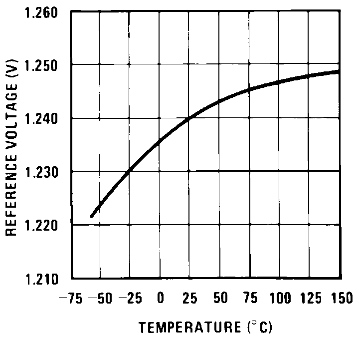 Figure 7. Temperature Stability
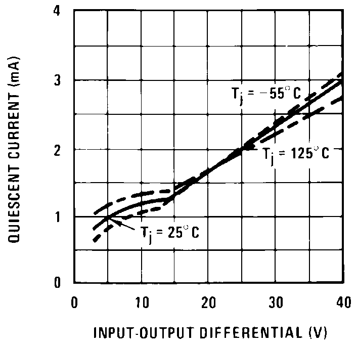 Figure 9. Minimum Operating Current
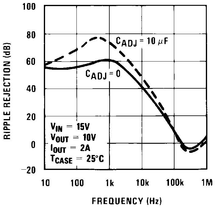 Figure 11. Ripple Rejection
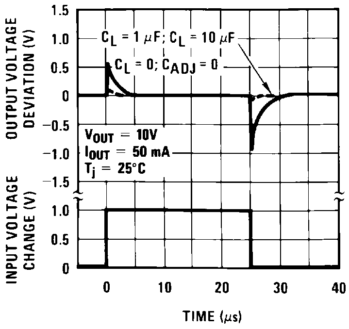 Figure 13. Line Transient Response
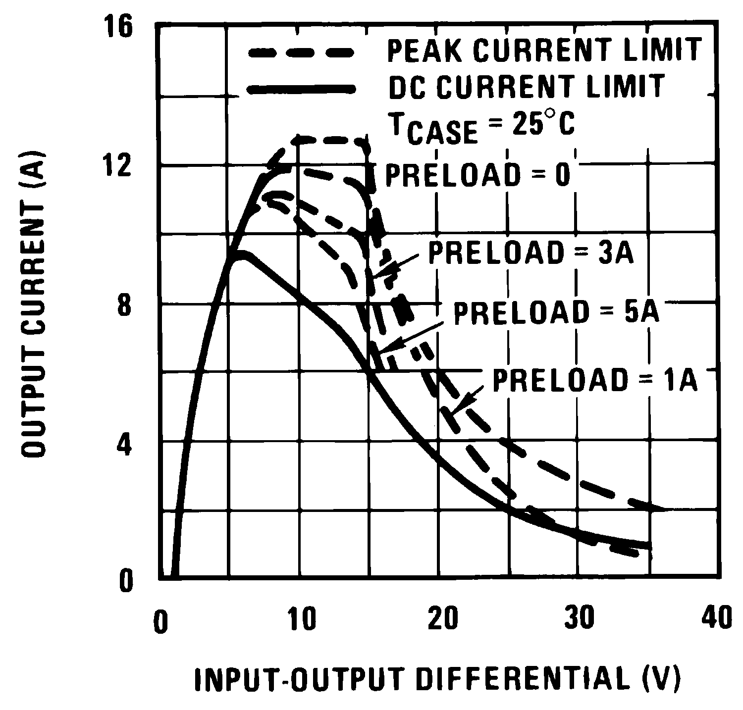 Figure 2. Current Limit
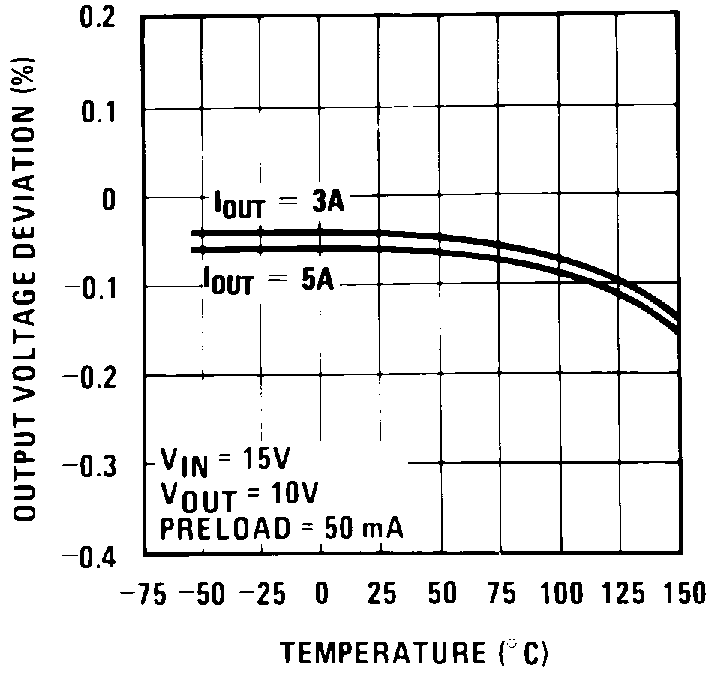 Figure 4. Load Regulation
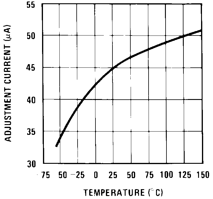 Figure 6. Adjustment Current
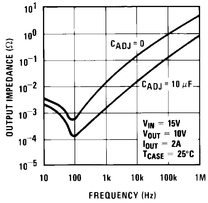 Figure 8. Output Impedance
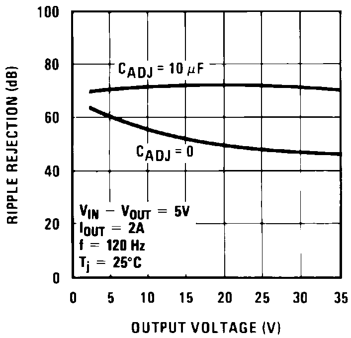 Figure 10. Ripple Rejection
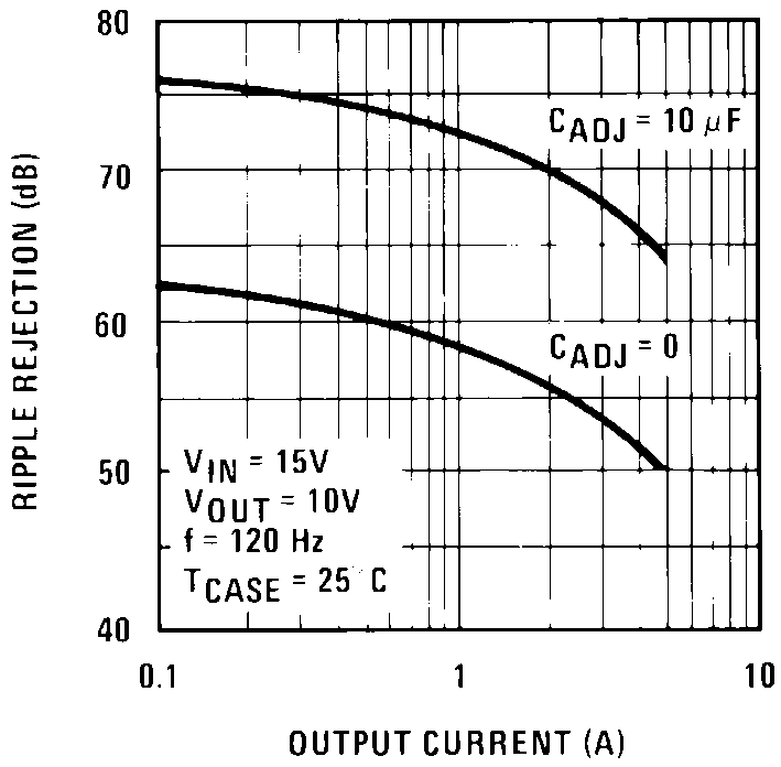 Figure 12. Ripple Rejection
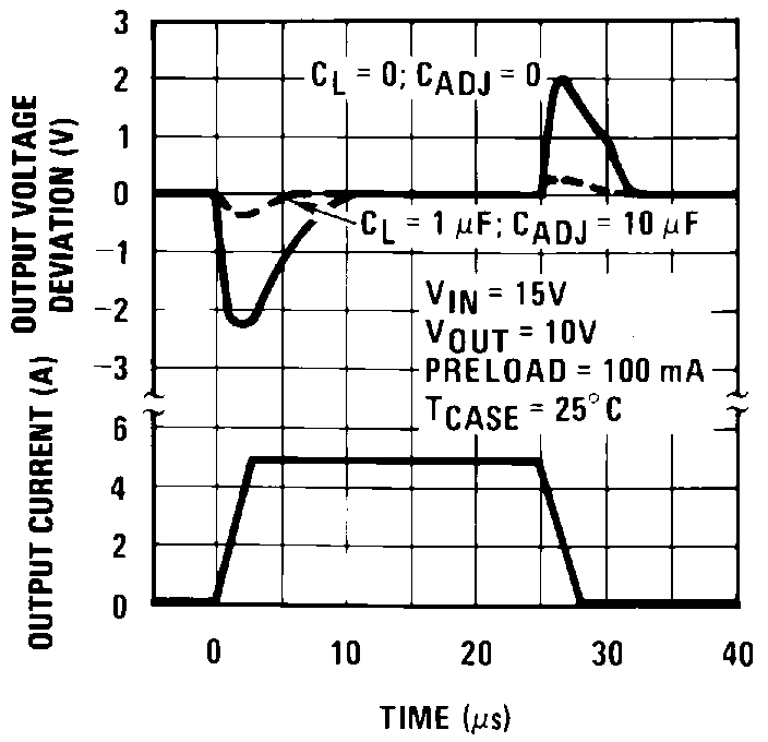 Figure 14. Load Transient Response