SNVS771C May   1998  – December 2016 LM138 , LM338

PRODUCTION DATA.  

  1. Features
  2. Applications
  3. Description
  4. Revision History
  5. Pin Configuration and Functions
  6. Specifications
    1. 6.1 Absolute Maximum Ratings
    2. 6.2 Recommended Operating Conditions
    3. 6.3 Thermal Information
    4. 6.4 Electrical Characteristics: LM138
    5. 6.5 Electrical Characteristics: LM338
    6. 6.6 Typical Characteristics
  7. Detailed Description
    1. 7.1 Overview
    2. 7.2 Functional Block Diagram
    3. 7.3 Feature Description
      1. 7.3.1 NPN Darlington Output Drive
      2. 7.3.2 Overload Block
      3. 7.3.3 Programmable Feedback
    4. 7.4 Device Functional Modes
      1. 7.4.1 Normal Operation
      2. 7.4.2 Operation With Low Input Voltage
      3. 7.4.3 Operation at Light Loads
      4. 7.4.4 Operation in Self Protection
  8. Application and Implementation
    1. 8.1 Application Information
    2. 8.2 Typical Applications
      1. 8.2.1 Constant 5-V Regulator
        1. 8.2.1.1 Design Requirements
        2. 8.2.1.2 Detailed Design Procedure
          1. 8.2.1.2.1 External Capacitors
          2. 8.2.1.2.2 Load Regulation
          3. 8.2.1.2.3 Protection Diodes
        3. 8.2.1.3 Application Curves
    3. 8.3 System Examples
  9. Power Supply Recommendations
  10. 10Layout
    1. 10.1 Layout Guidelines
    2. 10.2 Layout Example
  11. 11Device and Documentation Support
    1. 11.1 Receiving Notification of Documentation Updates
    2. 11.2 Related Links
    3. 11.3 Community Resources
    4. 11.4 Trademarks
    5. 11.5 Electrostatic Discharge Caution
    6. 11.6 Glossary
  12. 12Mechanical, Packaging, and Orderable Information

封装选项

机械数据 (封装 | 引脚)
散热焊盘机械数据 (封装 | 引脚)
订购信息

Pin Configuration and Functions

NDS Package
2-Pin TO-CAN
Bottom View
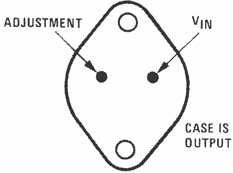
LM138 LM338 00906030.png
Package Number NDS0002A
NDE Package
3-Pin TO-220
Front View
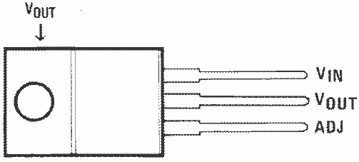
LM138 LM338 00906031.png
Package Number NDE0003B

Pin Functions

PIN I/O DESCRIPTION
NAME TO-220 TO-CAN
ADJ 1 1 I Output voltage adjustment pin. Connect to a resistor divider to set VO
VIN 3 2 I Supply input pin
VOUT 2 Case O Voltage output pin