SNOSBH7F April   1999  – September 2014 LF412-N

PRODUCTION DATA.  

  1. Features
  2. Applications
  3. Description
  4. Revision History
  5. Pin Configuration and Functions
  6. Specifications
    1. 6.1 Absolute Maximum Ratings
    2. 6.2 Handling Ratings
    3. 6.3 Recommended Operating Conditions
    4. 6.4 Thermal Information
    5. 6.5 DC Electrical Characteristics
    6. 6.6 AC Electrical Characteristics
    7. 6.7 Typical Characteristics
  7. Detailed Description
    1. 7.1 Overview
    2. 7.2 Functional Block Diagram
    3. 7.3 Feature Description
    4. 7.4 Device Functional Modes
      1. 7.4.1 Input and Output Stage
  8. Application and Implementation
    1. 8.1 Application Information
    2. 8.2 Typical Application
      1. 8.2.1 Design Requirements
      2. 8.2.2 Detailed Design Procedure
      3. 8.2.3 Application Curves
  9. Power Supply Recommendations
  10. 10Layout
    1. 10.1 Layout Guidelines
    2. 10.2 Layout Example
  11. 11Device and Documentation Support
    1. 11.1 Trademarks
    2. 11.2 Electrostatic Discharge Caution
    3. 11.3 Glossary
  12. 12Mechanical, Packaging, and Orderable Information

封装选项

机械数据 (封装 | 引脚)
散热焊盘机械数据 (封装 | 引脚)
订购信息

10 Layout

10.1 Layout Guidelines

As with most amplifiers, care should be taken with lead dress, component placement and supply decoupling in order to ensure stability. For example, resistors from the output to an input should be placed with the body close to the input to minimize “pick-up” and maximize the frequency of the feedback pole by minimizing the capacitance from the input to ground.

10.2 Layout Example

00915543.gif
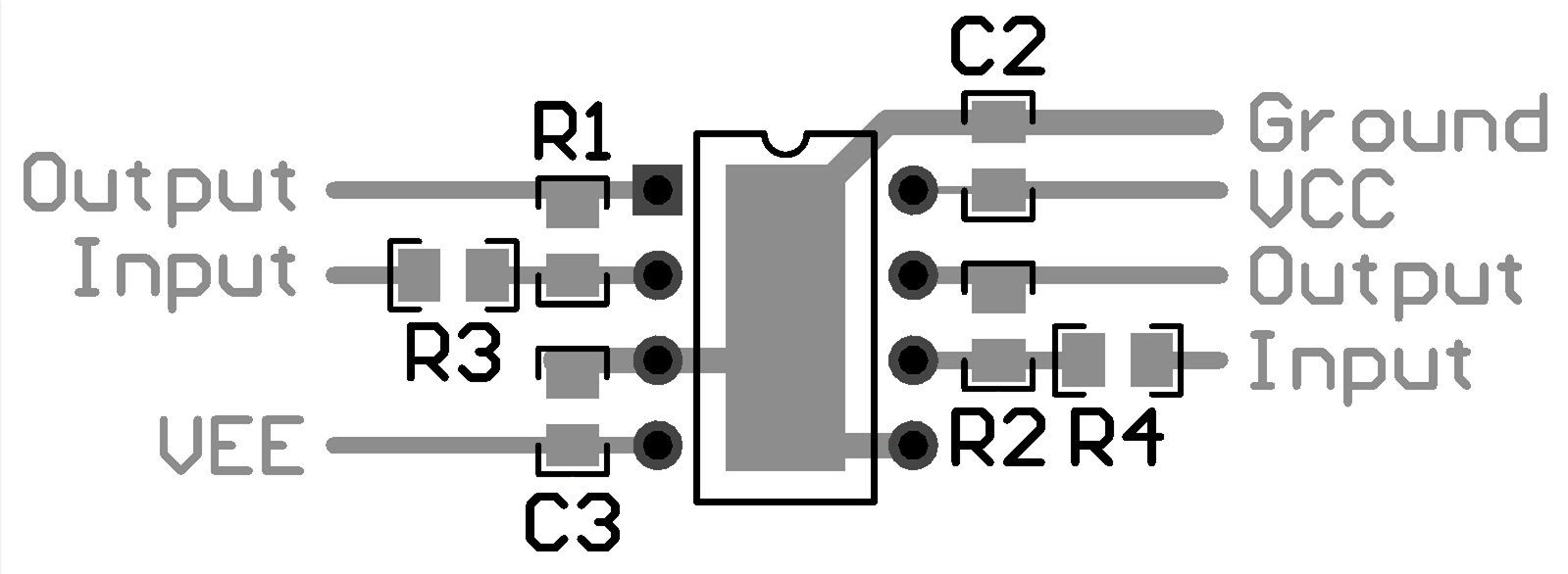
Figure 31. LF412 Layout