SNOSBH7F April 1999 – September 2014 LF412-N
PRODUCTION DATA.
7 Detailed Description
7.1 Overview
The LF412 devices are low cost, high speed, JFET input operational amplifiers with very low input offset voltage and input offset voltage drift. They require low supply current yet maintain a large gain bandwidth product and fast slew rate. In addition, well matched high voltage JFET input devices provide very low input bias and offset currents. The LF412-N dual is pin compatible with the LM1558, allowing designers to immediately upgrade the overall performance of existing designs.
These amplifiers may be used in applications such as high speed integrators, fast D/A converters, sample and hold circuits and many other circuits requiring low input offset voltage and drift, low input bias current, high input impedance, high slew rate and wide bandwidth.
7.2 Functional Block Diagram
 Figure 27. Each Amplifier
7.3 Feature Description
The amplifier's differential inputs consist of a non-inverting input (+IN) and an inverting input (-IN). The amplifier amplifies only the difference in voltage between the two inputs, which is called the differential input voltage. The output voltage of the op-amp VOUT is given by the equation VOUT = AOL(IN+ - IN-).
7.4 Device Functional Modes
7.4.1 Input and Output Stage
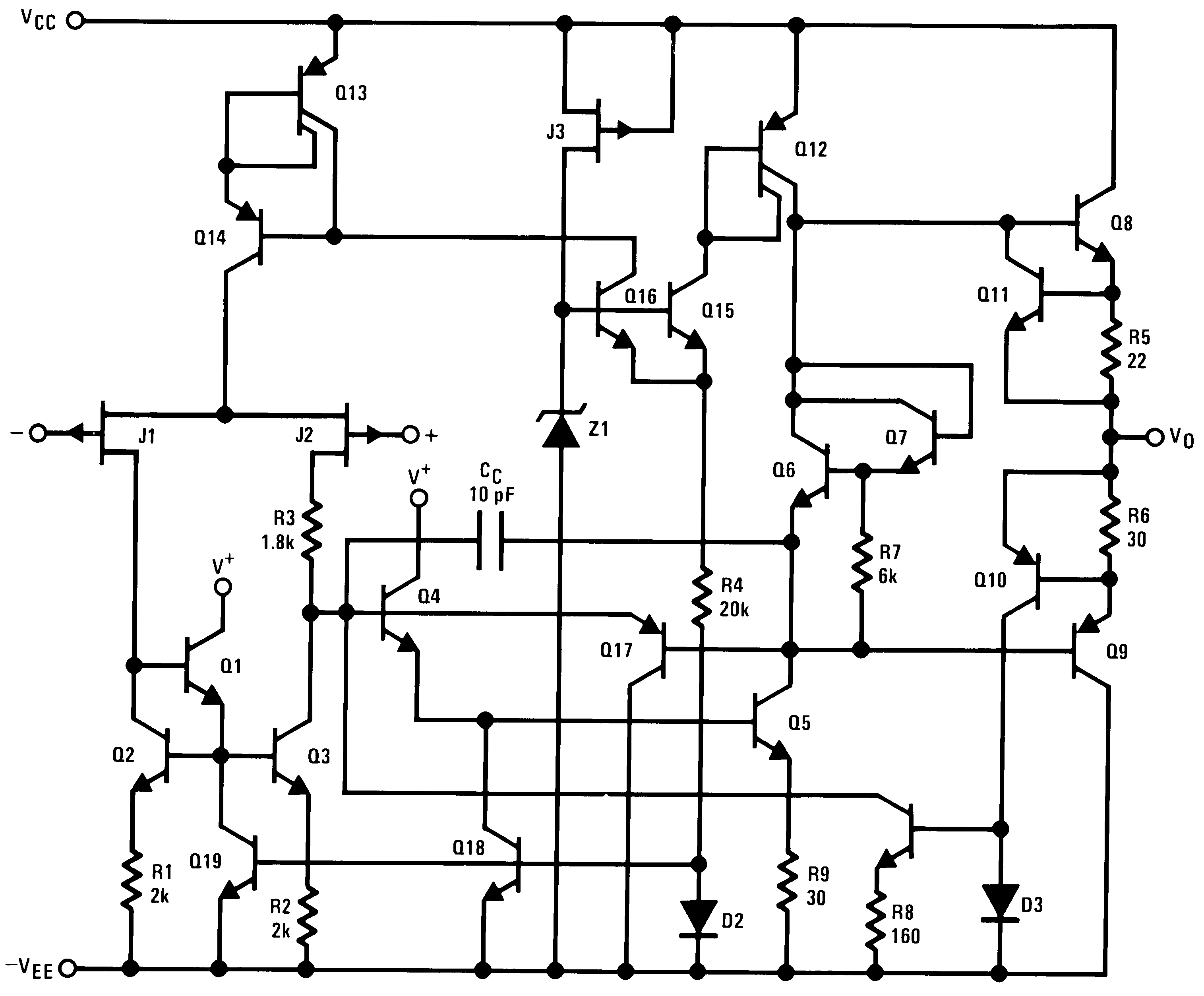 Figure 28. 1/2 Dual LF412