ZHCSAK0C July 2008 – December 2015 INA333
PRODUCTION DATA.
- 1 特性
- 2 应用范围
- 3 说明
- 4 修订历史记录
- 5 Pin Configuration and Functions
- 6 Specifications
- 7 Detailed Description
- 8 Application and Implementation
- 9 Power Supply Recommendations
- 10Layout
- 11器件和文档支持
- 12机械、封装和可订购信息
封装选项
机械数据 (封装 | 引脚)
散热焊盘机械数据 (封装 | 引脚)
订购信息
10 Layout
10.1 Layout Guidelines
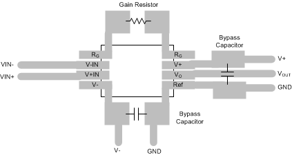
Attention to good layout practices is always recommended. Keep traces short and, when possible, use a printed-circuit-board (PCB) ground plane with surface-mount components placed as close to the device pins as possible. Place a 0.1-μF bypass capacitor closely across the supply pins. These guidelines should be applied throughout the analog circuit to improve performance and provide benefits such as reducing the electromagnetic-interference (EMI) susceptibility.
Instrumentation amplifiers vary in the susceptibility to radio-frequency interference (RFI). RFI can generally be identified as a variation in offset voltage or DC signal levels with changes in the interfering RF signal. The INA333 device has been specifically designed to minimize susceptibility to RFI by incorporating passive RC filters with an 8-MHz corner frequency at the VIN+ and VIN– inputs. As a result, the INA333 device demonstrates remarkably low sensitivity compared to previous generation devices. Strong RF fields may continue to cause varying offset levels, however, and may require additional shielding.
10.2 Layout Example
 Figure 40. INA333 Layout