ZHCSG76 April 2017 INA233
PRODUCTION DATA.
- 1 特性
- 2 应用范围
- 3 说明
- 4 修订历史记录
- 5 Pin Configuration and Functions
- 6 Specifications
-
7 Detailed Description
- 7.1 Overview
- 7.2 Functional Block Diagram
- 7.3 Feature Description
- 7.4 Device Functional Modes
- 7.5 Programming
- 7.6
Register Maps
- 7.6.1 PMBus Command Support
- 7.6.2
Standard PMBus Commands
- 7.6.2.1 CLEAR_FAULTS (03h)
- 7.6.2.2 RESTORE_DEFAULT_ALL (12h)
- 7.6.2.3 CAPABILITY (19h)
- 7.6.2.4 IOUT_OC_WARN_LIMIT (4Ah) [default = 01111111 11111000]
- 7.6.2.5 VIN_OV_WARN_LIMIT (57h) [default = 01111111 11111000]
- 7.6.2.6 VIN_UV_WARN_LIMIT (58h) [default = 00000000 00000000]
- 7.6.2.7 PIN_OP_WARN_LIMIT (6Bh) [default = 11111111 11110000]
- 7.6.2.8 STATUS_BYTE (78h)
- 7.6.2.9 STATUS_WORD (79h)
- 7.6.2.10 STATUS_IOUT (7Bh)
- 7.6.2.11 STATUS_INPUT (7Ch)
- 7.6.2.12 STATUS_CML (7Eh)
- 7.6.2.13 STATUS_MFR_SPECIFIC (80h)
- 7.6.2.14 READ_EIN (86h)
- 7.6.2.15 READ_VIN (88h)
- 7.6.2.16 READ_IIN (89h)
- 7.6.2.17 READ_VOUT (8Bh)
- 7.6.2.18 READ_IOUT (8Ch, R)
- 7.6.2.19 READ_POUT (96h, R)
- 7.6.2.20 READ_PIN (97h, R)
- 7.6.2.21 MFR_ID (99h)
- 7.6.2.22 MFR_MODEL (9Ah)
- 7.6.2.23 MFR_REVISION (9Bh)
- 7.6.3
Manufacturer-Specific PMBus Commands
- 7.6.3.1 MFR_ADC_CONFIG (D0h) [default = 01000001 00100111]
- 7.6.3.2 MFR_READ_VSHUNT (D1h) [default = 00000000 00000000]
- 7.6.3.3 MFR_ALERT_MASK (D2h) [default = XXXXXXXX 11110000]
- 7.6.3.4 MFR_CALIBRATION (D4h) [default = 00000000 00000001]
- 7.6.3.5 MFR_DEVICE_CONFIG (D5h) [default = 00000010]
- 7.6.3.6 5.1.1 CLEAR_EIN (D6h)
- 7.6.3.7 TI_MFR_ID (E0h) [value = 01010100 01001001]
- 7.6.3.8 TI_MFR_MODEL (E1h) [value = 00110011 00110011]
- 7.6.3.9 TI_MFR_REVISION (E2h) [value = 01000001 00110000]
- 8 Application and Implementation
- 9 Power Supply Recommendations
- 10Layout
- 11器件和文档支持
- 12机械、封装和可订购信息
8 Application and Implementation
NOTE
Information in the following applications sections is not part of the TI component specification, and TI does not warrant its accuracy or completeness. TI’s customers are responsible for determining suitability of components for their purposes. Validate and test the design implementation to confirm system functionality.
8.1 Application Information
The INA233 is a current shunt and power monitor with an I2C-, SMBus-, and PMBus-compatible interface. The device monitors both a shunt voltage drop and bus supply voltage. Programmable calibration value, conversion times, and averaging (combined with an internal multiplier) enable direct readouts of current in amperes and power in watts.
8.2 Typical Application
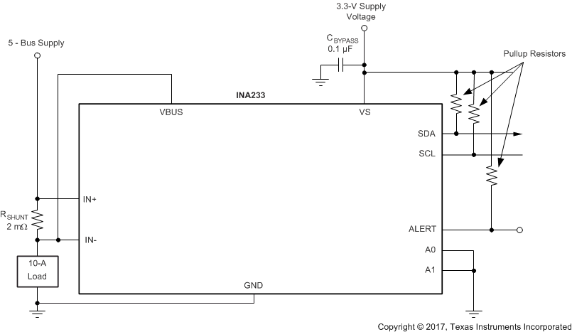
 Figure 43. Typical High-Side Sensing Circuit Configuration, INA233
8.2.1 Design Requirements
The INA233 measures the voltage developed across a current-sensing resistor (RSHUNT) when current passes through it. The device also measures the bus supply voltage and can calculate power when the calibration register is properly configured. The device comes with alert capability where the ALERT pin can be programmed to respond to a user-defined event or to a conversion ready notification. This design illustrates the ability of the ALERT pin to respond to a set input overvoltage threshold and how to correctly set the calibration registers and calculate returned values. Table 35 details the requirements for this design.
Table 35. Design Requirements
| PARAMETER | DESIGN TARGET |
|---|---|
| Power-supply voltage, VS | 5 V |
| Nominal bus supply voltage, VBUS | 5 V |
| VBUS overvoltage warning threshold | 5.5 V |
| Nominal load current | 10 A |
| Peak load current | 15 A |
| Overcurrent warning threshold | 15 A |
| RSHUNT | 2 mΩ |
8.2.2 Detailed Design Procedure
This design example walks through the process of programming the calibration register, calculating the PMBus coefficients, setting the correct overvoltage and overcurrent warning thresholds, and how to properly scale returned values from the device. The device alert response time is also examined with 140-µs and 1.1-ms ADC conversion rates.
8.2.2.1 Programming the Calibration Register
For this example, assuming a peak current of less than 15 A, the Current_LSB is calculated to be 457.7 μA/bit using Equation 2. Selecting a value for the Current_LSB of 500 μA/bit or 1 mA/bit significantly simplifies the conversion of the returned value from the READ_IN and READ_PIN commands to amperes and watts. For this example, a value of 1 mA/bit is chosen for the Current_LSB. Using this value for the Current_LSB does trade a small amount of resolution for having a simpler conversion process on the user side. Using Equation 1 in this example with a Current_LSB value of 1 mA/bit and a shunt resistor of 2 mΩ results in a MFR_CALIBRATION register value of 2560d (or A00h).
8.2.2.2 Calculating PMBus Coefficients
The m, b, and R coefficients are fixed for bus voltage measurements returned by the READ_VIN and READ_VOUT and are available from Table 1.
For current and power measurements, the value for the m and R coefficients must be calculated. For current measurements returned by the READ_IIN and READ_IOUT commands, the value for m is calculated by inverting the Current_LSB used to set the MFR_CALIBRATION register and shifting the decimal location if needed to minimize rounding errors. In this example, using the Current_LSB of 1 mA/bit, the value of m is calculated to be 1000. Shifting the decimal location does not obtain higher accuracy because the value for m is a whole number. The value for R in this example is 0 because the decimal location for the value of m does not need shifting.
The POWER_LSB value is 25 times the value of the CURRENT_LSB, therefore, the value for m is reduced by a factor of 25. For this example, the value for the m power coefficient 1000 / 25 or 40. For this case, the R coefficient is also 0 because m is a whole number. If m is not a whole number, then shifting the decimal place is advantageous to reduce rounding errors while keeping the value between –32768 and 32767. Decimal shifts to the right result in negative values for R and shifts to the left result in positive values; the number of shifts is the absolute value of R.
The value of 0 can be used for b for both current and power measurements with very little loss in accuracy because the offset for power and current measurements is very low. The m, b, and R coefficients are fixed for bus voltage measurements returned by the READ_VIN and READ_VOUT and are available from Table 1.
8.2.2.3 Programming Warning Thresholds
Warning thresholds are set by converting the warning value from volts, amperes, and watts to the appropriate digital word using Equation 4 with the correct values for m, b, and R. For example, to set a bus voltage overvoltage warning at 5.5 V with the VIN_OV_WARN_LIMIT command, the correct value to write with this command is 4400d or 1130h. The least significant last three bits of the 16-bit word are hard coded to 0 because the warning thresholds only have 12 bits of effective resolution. For this example there is no change to what is written in the VIN_OV_WARN_LIMIT register because the last three bits are already zero. To set an overcurrent warning level at 15 A with the IIN_OC_WARN_LIMIT command, the correct value to write to the device is 15000d (or 3A98h).
8.2.2.4 Calculating Returned Telemetry Values
When the value for the m, b, and R coefficients are known, returned values can be translated to volts, amperes, or watts by using Equation 3 with the calculated m, b, and R coefficients. Alternatively, returned values can be calculated by multiplying the returned code by the corresponding LSB size as discussed in the Calibration Register and Scaling section.
8.2.3 Application Curves
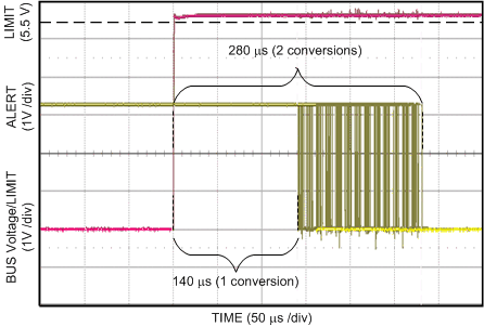
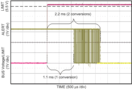
Figure 44 shows the ALERT pin response to a bus overvoltage limit of 5.6 V for a conversion time (tCT) of 1.1 ms and averaging set to 1. Figure 45 shows the response for the same limit but with the conversion time reduced to 140 µs. For the scope shots shown in these figures, persistence was enabled on the ALERT channel. Figure 44 and Figure 45 show how the ALERT response time can vary depending on when the fault condition occurs relative to the internal ADC clock of the INA233. For fault conditions that are just exceeding the limit threshold, the response time for the ALERT pin can vary from one to two conversion cycles. As mentioned previously, the variation is because of the timing on when the fault event occurs relative to the start time of the internal ADC conversion cycle. For fault events that greatly exceed the limit threshold, the alert can respond in less than one conversion cycle because fewer samples are required for the average to exceed the limit threshold value.

