SBOS501F January 2010 – February 2015 INA128-HT , INA129-HT
PRODUCTION DATA.
- 1 Features
- 2 Applications
- 3 Description
- 4 Simplified Schematic
- 5 Revision History
- 6 Pin Configuration and Functions
- 7 Specifications
- 8 Detailed Description
- 9 Application and Implementation
- 10Power Supply Recommendations
- 11Layout
- 12Device and Documentation Support
- 13Mechanical, Packaging, and Orderable Information
封装选项
机械数据 (封装 | 引脚)
散热焊盘机械数据 (封装 | 引脚)
订购信息
7 Specifications
7.1 Absolute Maximum Ratings
over operating free-air temperature range (unless otherwise noted) (1)| MIN | MAX | UNIT | |||
|---|---|---|---|---|---|
| Volttage | Supply | ±18 | V | ||
| Analog input | ±40 | ||||
| Current | Output short-circuit (to ground) | Continuous | |||
| Operating temperature | HKJ, HKQ, KGD and JD packages | –55 | 210 | °C | |
| D package | –55 | 175 | |||
| Storage temperature, Tstg | HKJ, HKQ, KGD and JD packages | –55 | 210 | °C | |
| D package | –55 | 175 | |||
(1) Stresses beyond those listed under Absolute Maximum Ratings may cause permanent damage to the device. These are stress ratings only, which do not imply functional operation of the device at these or any other conditions beyond those indicated under Recommended Operating Conditions. Exposure to absolute-maximum-rated conditions for extended periods may affect device reliability.
7.2 ESD Ratings
| VALUE | UNIT | |||
|---|---|---|---|---|
| A. INA218-HT (D, HKJ, or JDJ Package) | ||||
| V(ESD) | Electrostatic discharge | Human-body model (HBM), per ANSI/ESDA/JEDEC JS-001(1) | ±2000 | V |
| Charged-device model (CDM), per JEDEC specification JESD22-C101(2) | ±50 | |||
| B. INA129-HT (HKQ Package) | ||||
| V(ESD) | Electrostatic discharge | Human-body model (HBM), per ANSI/ESDA/JEDEC JS-001(1) | ±4000 | V |
| Charged-device model (CDM), per JEDEC specification JESD22-C101(2) | ±200 | |||
(1) JEDEC document JEP155 states that 500-V HBM allows safe manufacturing with a standard ESD control process.
(2) JEDEC document JEP157 states that 250-V CDM allows safe manufacturing with a standard ESD control process.
7.3 Recommended Operating Conditions
over operating free-air temperature range (unless otherwise noted)| MIN | NOM | MAX | UNIT | ||
|---|---|---|---|---|---|
| V power supply | ±2.25 | ±15 | ±18 | V | |
| Input common-mode voltage range for VO = 0 | V - 2 V | V + –2 V | |||
| TA operating temperature INA128-HT | –55 | 175 | °C | ||
| TA operating temperature INA129-HT | –55 | 210 | °C | ||
7.4 Thermal Information: INA128-HT
| THERMAL METRIC(1) | INA128-HT | UNIT | |
|---|---|---|---|
| D [SOIC] | |||
| 8 PINS | |||
| RθJA | Junction-to-ambient thermal resistance | 110 | °C/W |
| RθJC(top) | Junction-to-case (top) thermal resistance | 57 | |
| RθJB | Junction-to-board thermal resistance | 54 | |
| ψJT | Junction-to-top characterization parameter | 11 | |
| ψJB | Junction-to-board characterization parameter | 53 | |
(1) For more information about traditional and new thermal metrics, see the IC Package Thermal Metrics application report, SPRA953.
7.5 Electrical Characteristics: INA128-HT
over operating free-air temperature range (unless otherwise noted)| PARAMETER | TEST CONDITIONS |
TA = –55°C to +125°C | TA = 175°C(1) | UNIT | |||||||
|---|---|---|---|---|---|---|---|---|---|---|---|
| MIN | TYP | MAX | MIN | TYP | MAX | ||||||
| INPUT | |||||||||||
| OFFSET VOLTAGE, RTI | |||||||||||
| Initial | TA = 25°C | ±25 ±100/G |
±125 ±1000/G |
µV | |||||||
| vs temperature | TA = TMIN to TMAX | ±0.2 ±5/G |
±1 ±20/G |
±3.5 ±80/G |
µV/°C | ||||||
| vs power supply | VS = ±2.25 V to ±18 V |
±2 ±200/G |
±5 ±500/G |
µV/V | |||||||
| Long-term stability | ±1 ±3/G | ±1 ±3/G | µV/mo | ||||||||
| Impedance, differential | 1010 || 2 | 1010 || 2 | Ω || pF | ||||||||
| Common mode | 1011||9 | 1011||9 | Ω || pF | ||||||||
| Common mode voltage range(2) | VO = 0 V | (V+) − 2 | (V+) − 1.4 | (V+) − 2 | (V+) − 1.4 | V | |||||
| (V−) + 2 | (V−) + 1.7 | (V−) + 2 | (V−) + 1.7 | V | |||||||
| Safe input voltage | ±40 | ±40 | V | ||||||||
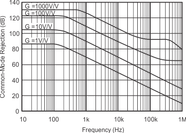
| Common-mode rejection | VCM = ±13 V, ΔRS = 1 kΩ |
||||||||||
| G = 1 | 58 | 86 | 58 | 75 | dB | ||||||
| G = 10 | 78 | 106 | 78 | 85 | |||||||
| G = 100 | 99 | 125 | 99 | 110 | |||||||
| G = 1000 | 113 | 130 | 113 | 120 | |||||||
| CURRENT | |||||||||||
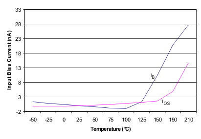
| Bias current | ±2 | ±10 | ±45 | nA | |||||||
| vs temperature | ±30 | ±550 | pA/°C | ||||||||
| Offset Current | ±1 | ±10 | ±45 | nA | |||||||
| vs temperature | ±30 | ±550 | pA/°C | ||||||||
| NOISE | |||||||||||
| Noise voltage, RTI | G = 1000, RS = 0 Ω |
||||||||||
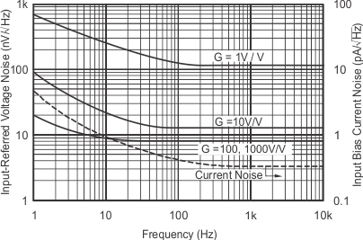
| f = 10 Hz | 10 | 10 | nV/√Hz | ||||||||
| f = 100 Hz | 8 | 8 | nV/√Hz | ||||||||
| f = 1 kHz | 8 | 8 | nV/√Hz | ||||||||
| fB = 0.1 Hz to 10 Hz | 0.2 | 0.8 | µVPP | ||||||||
| Noise current | |||||||||||
| f = 10 Hz | 0.9 | pA/√Hz | |||||||||
| f = 1 kHz | 0.3 | pA/√Hz | |||||||||
| fB = 0.1 Hz to 10 Hz | 30 | pAPP | |||||||||
| GAIN | |||||||||||
| Gain equation | 1 + (50 kΩ/RG) |
1 + (50 kΩ/RG) |
V/V | ||||||||
| Range of gain | 1 | 10000 | 1 | 10000 | V/V | ||||||
| Gain error | G = 1 | ±0.01 | ±0.1 | ±0.1% | ±0.5% | ||||||
| G = 10 | ±0.02 | ±0.5 | ±0.5% | ±1% | |||||||
| G = 100 | ±0.05 | ±0.7 | ±0.7% | ±1.5% | |||||||
| G = 1000 | ±0.5 | ±2.5 | ±2% | ±4% | |||||||
| Gain vs temperature(3) | G = 1 | ±1 | ±10 | ±75 | ppm/°C | ||||||
| 50-kΩ resistance(3)(4) | ±25 | ±100 | ±75 | ppm/°C | |||||||
| Nonlinearity | VO = ±13.6 V, G = 1 |
±0.0001 | ±0.001 | ±0.008 | % of FSR | ||||||
| G = 10 | ±0.0003 | ±0.002 | ±0.01 | ||||||||
| G = 100 | ±0.0005 | ±0.002 | ±0.01 | ||||||||
| G = 1000 | ±0.001 | See (5) | ±0.6 | See (5) | |||||||
| OUTPUT | |||||||||||
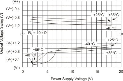
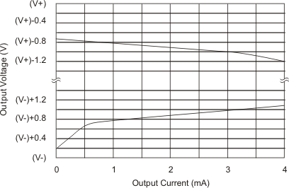
| Voltage | Positive | RL = 10 kΩ | (V+) − 1.4 | (V+) − 0.9 | (V+) − 1.4 | (V+) − 0.9 | V | ||||
| Negative | RL = 10 kΩ | (V−) + 1.4 | (V−) + 0.8 | (V−) + 1.4 | (V−) + 0.8 | ||||||
| Load capacitance stability | 1000 | 1000 | pF | ||||||||
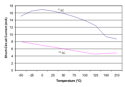
| Short-circuit current | +6/−15 | +6/−15 | mA | ||||||||
| FREQUENCY RESPONSE | |||||||||||
| Bandwidth, −3 dB | G = 1 | 1300 | 1100 | kHz | |||||||
| G = 10 | 700 | 700 | |||||||||
| G = 100 | 200 | 190 | |||||||||
| G = 1000 | 20 | 17.5 | |||||||||
| Slew rate | VO = ±10 V, G = 10 |
4 | 4 | V/µs | |||||||
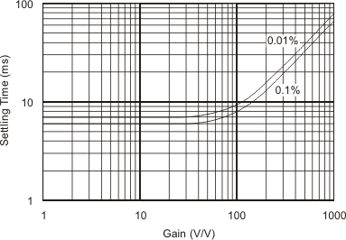
| Settling time, 0.01% | G = 1 | 7 | 7 | µs | |||||||
| G = 10 | 7 | 7 | |||||||||
| G = 100 | 9 | 9 | |||||||||
| G = 1000 | 80 | 80 | |||||||||
| Overload recovery | 50% overdrive | 4 | 4 | µs | |||||||
| POWER SUPPLY | |||||||||||
| Voltage range | ±2.25 | ±15 | ±18 | ±2.25 | ±15 | ±18 | V | ||||
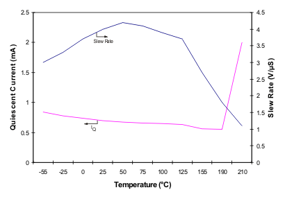
| Current, total | VIN = 0 V | ±0.7 | ±1 | ±1 | mA | ||||||
| TEMPERATURE RANGE | |||||||||||
| Specification | −55 | +125 | 175 | °C | |||||||
| Operating | −55 | +125 | 175 | °C | |||||||
(1) Minimum and maximum parameters are characterized for operation at TA = 175°C, but may not be production tested at that temperature. Production test limits with statistical guardbands are used to ensure high temperature performance.
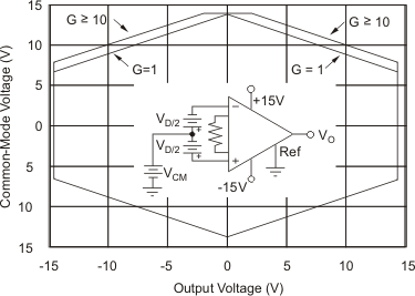
(2) Input common-mode range varies with output voltage — see typical curves.
(3) Specified by wafer test.
(4) Temperature coefficient of the 50-kΩ term in the gain equation.
(5) Nonlinearity measurements in G = 1000 are dominated by noise. Typical nonlinearity is ±0.001%.
7.6 Electrical Characteristics: INA129-HT
over operating free-air temperature range (unless otherwise noted)| PARAMETER | TEST CONDITIONS |
TA = –55°C to +125°C | TA = 210°C(1) | UNIT | |||||||
|---|---|---|---|---|---|---|---|---|---|---|---|
| MIN | TYP | MAX | MIN | TYP | MAX | ||||||
| INPUT | |||||||||||
| OFFSET VOLTAGE, RTI | |||||||||||
| Initial | TA = 25°C | ±25 ±100/G |
±125 ±1000/G |
µV | |||||||
| vs temperature | TA = TMIN to TMAX | ±0.2 ±5/G |
±1 ±20/G |
±1 ±850/G |
µV/°C | ||||||
| vs power supply | VS = ±2.25 V to ±18 V |
±0.2 ±20/G |
±2 ±200/G |
±20 ±1000/G |
µV/V | ||||||
| Long-term stability | ±1 ±3/G | ±1 ±3/G | µV/mo | ||||||||
| Impedance, differential | 1010 || 2 | 1010 || 2 | Ω || pF | ||||||||
| Common mode | 1011||9 | 1011||9 | Ω || pF | ||||||||
| Common mode voltage range(2) | VO = 0 V | (V+) − 2 | (V+) − 1.4 | (V+) − 2 | (V+) − 1.4 | V | |||||
| (V−) + 2 | (V−) + 1.7 | (V−) + 2 | (V−) + 1.7 | V | |||||||
| Safe input voltage | ±40 | ±40 | V | ||||||||
| Common-mode rejection | VCM = ±13 V, ΔRS = 1 kΩ |
||||||||||
| G = 1 | 58 | 86 | 53 | dB | |||||||
| G = 10 | 78 | 106 | 69 | ||||||||
| G = 100 | 99 | 125 | 89 | ||||||||
| G = 1000 | 113 | 130 | 95 | ||||||||
| CURRENT | |||||||||||
| Bias current | ±2 | ±10 | ±50 | nA | |||||||
| vs temperature | ±30 | ±600 | pA/°C | ||||||||
| Offset Current | ±1 | ±10 | ±50 | nA | |||||||
| vs temperature | ±30 | ±600 | pA/°C | ||||||||
| NOISE | |||||||||||
| Noise voltage, RTI | G = 1000, RS = 0 Ω |
||||||||||
| f = 10 Hz | 10 | 25 | nV/√Hz | ||||||||
| f = 100 Hz | 8 | 20 | nV/√Hz | ||||||||
| f = 1 kHz | 8 | 20 | nV/√Hz | ||||||||
| fB = 0.1 Hz to 10 Hz | 0.2 | 2 | µVPP | ||||||||
| Noise current | |||||||||||
| f = 10 Hz | 0.9 | pA/√Hz | |||||||||
| f = 1 kHz | 0.3 | pA/√Hz | |||||||||
| fB = 0.1 Hz to 10 Hz | 30 | pAPP | |||||||||
| GAIN | |||||||||||
| Gain equation | 1 + (49.4 kΩ/RG) |
1 + (49.4 kΩ/RG) |
V/V | ||||||||
| Range of gain | 1 | 10000 | 1 | 10000 | V/V | ||||||
| Gain error | G = 1 | ±0.01% | ±0.1% | ±1.1% | |||||||
| G = 10 | ±0.02% | ±0.5% | ±2.6% | ||||||||
| G = 100 | ±0.05% | ±0.7% | ±13.5% | ||||||||
| G = 1000 | ±0.5% | ±2.5% | ±65.5% | ||||||||
| Gain vs temperature(3) | G = 1 | ±1 | ±10 | ±100 | ppm/°C | ||||||
| 49.4-kΩ resistance(3)(4) | ±25 | ±100 | ±100 | ppm/°C | |||||||
| Nonlinearity | VO = ±13.6 V, G = 1 |
±0.0001 | ±0.001 | ±0.1 | % of FSR | ||||||
| G = 10 | ±0.0003 | ±0.002 | ±0.2 | ||||||||
| G = 100 | ±0.0005 | ±0.002 | ±0.7 | ||||||||
| G = 1000 | ±0.001 | See (5) | ±2.4 | See (5) | |||||||
| OUTPUT | |||||||||||
| Voltage | Positive | RL = 10kΩ | (V+) − 1.4 | (V+) − 0.9 | (V+) − 1.4 | (V+) − 0.9 | V | ||||
| Negative | RL = 10kΩ | (V−) + 1.4 | (V−) + 0.8 | (V−) + 1.4 | (V−) + 0.8 | ||||||
| Load capacitance stability | 1000 | 1000 | pF | ||||||||
| Short-curcuit current | +6/−15 | +12/−5 | mA | ||||||||
| FREQUENCY RESPONSE | |||||||||||
| Bandwidth, −3 dB | G = 1 | 1300 | 850 | kHz | |||||||
| G = 10 | 700 | 400 | |||||||||
| G = 100 | 200 | 50 | |||||||||
| G = 1000 | 20 | 7.5 | |||||||||
| Slew rate | VO = ±10 V, G = 10 |
4 | 4 | V/µs | |||||||
| Settling time, 0.01% | G = 1 | 7 | 10 | µs | |||||||
| G = 10 | 7 | 10 | |||||||||
| G = 100 | 9 | 30 | |||||||||
| G = 1000 | 80 | 150 | |||||||||
| Overload recovery | 50% overdrive | 4 | 4 | µs | |||||||
| POWER SUPPLY | |||||||||||
| Voltage range | ±2.25 | ±15 | ±18 | ±2.25 | ±15 | ±18 | V | ||||
| Current, total | VIN = 0 V | ±0.7 | ±1 | ±2 | mA | ||||||
| TEMPERATURE RANGE | |||||||||||
| Specification | −55 | +125 | 210 | °C | |||||||
| Operating | −55 | +125 | 210 | °C | |||||||
(1) Minimum and maximum parameters are characterized for operation at TA = 210°C, but may not be production tested at that temperature. Production test limits with statistical guardbands are used to ensure high temperature performance.
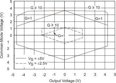
(2) Input common-mode range varies with output voltage — see typical curves.
(3) Specified by wafer test.
(4) Temperature coefficient of the 49.4-kΩ term in the gain equation.
(5) Nonlinearity measurements in G = 1000 are dominated by noise. Typical nonlinearity is ±0.001%.
1. See the data sheet for absolute maximum and minimum recommended operating conditions.
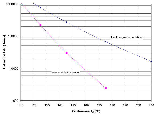
2. The predicted operating lifetime vs. junction temperature is based on reliability modeling using electromigration as the dominant failure mechanism affecting device wearout for the specific device process and design characterisitics.
3. Wirebond lifetime is only applicable for D package.
Figure 1. INA128HD, INA129SKGD1, and INA129SKGD2 Operating Life Derating Chart
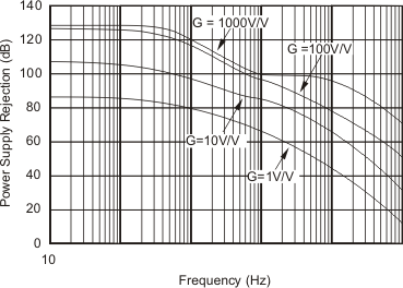
7.7 Typical Characteristics
At TA = 25°C, VS = ±15 V, unless otherwise noted.
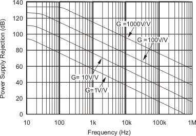
| VS = ±15 V | ||
| VS = ±5 V, ±2.5 V | ||
