SNLS026D March 2000 – June 2016 DS90LV027A
PRODUCTION DATA.
- 1 Features
- 2 Applications
- 3 Description
- 4 Revision History
- 5 Pin Configuration and Functions
- 6 Specifications
- 7 Parameter Measurement Information
- 8 Detailed Description
- 9 Application and Implementation
- 10Power Supply Recommendations
- 11Layout
- 12Device and Documentation Support
- 13Mechanical, Packaging, and Orderable Information
1 Features
- >600-Mbps (300 MHz) Switching Rates
- 0.3-ns Typical Differential Skew
- 0.7-ns Maximum Differential Skew
- 1.5-ns Maximum Propagation Delay
- 3.3-V Power Supply Design
- ±360-mV Differential Signaling
- Low Power Dissipation (46 mW at 3.3-V Static)
- Flow-Through Design Simplifies PCB Layout
- Interoperable With Existing 5-V LVDS Devices
- Power-Off Protection (Outputs in High Impedance)
- Conforms to TIA/EIA-644 Standard
- 8-Pin SOIC Package Saves Space
- Industrial Temperature Operating Range: −40°C to 85°C
2 Applications
- Multi-Function Printers
- LVCMOS-to-LVDS Translation
- Building and Factory Automation
- Grid Infrastructure
3 Description
The DS90LV027A is a dual LVDS driver device optimized for high data rate and low-power applications. The device is designed to support data rates in excess of 600 Mbps (300 MHz) using Low Voltage Differential Signaling (LVDS) technology. The DS90LV027A is a current mode driver allowing power dissipation to remain low even at high frequency. In addition, the short circuit fault current is also minimized.
The device is in a 8-pin SOIC package. The DS90LV027A has a flow-through design for easy printed-circuit board (PCB) layout. The differential driver outputs provides low EMI with its typical low output swing of 360 mV. It is perfect for high-speed transfer of clock and data. The DS90LV027A can be paired with its companion dual line receiver, the DS90LV028A, or with any of TI's LVDS receivers, to provide a high-speed point-to-point LVDS interface.
Device Information(1)
| PART NUMBER | PACKAGE | BODY SIZE (NOM) |
|---|---|---|
| DS90LV027A | SOIC (8) | 4.90 mm × 3.91 mm |
- For all available packages, see the orderable addendum at the end of the data sheet.
space
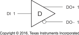
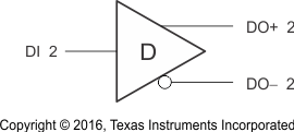
Functional Diagrams

