ZHCSDY8C June 2015 – August 2017 DRV8880
PRODUCTION DATA.
- 1 特性
- 2 应用
- 3 说明
- 4 修订历史记录
- 5 Pin Configuration and Functions
- 6 Specifications
-
7 Detailed Description
- 7.1 Overview
- 7.2 Functional Block Diagram
- 7.3
Feature Description
- 7.3.1 Stepper Motor Driver Current Ratings
- 7.3.2 PWM Motor Drivers
- 7.3.3 Microstepping Indexer
- 7.3.4 Current Regulation
- 7.3.5
Decay Modes
- 7.3.5.1 Mode 1: Slow Decay for Increasing and Decreasing Current
- 7.3.5.2 Mode 2: Slow Decay for Increasing Current, Mixed Decay for Decreasing current
- 7.3.5.3 Mode 3: Mixed Decay for Increasing and Decreasing Current
- 7.3.5.4 Mode 4: Slow Decay for Increasing Current, Fast Decay for Decreasing current
- 7.3.5.5 Mode 5: Fast Decay for Increasing and Decreasing Current
- 7.3.6 AutoTune
- 7.3.7 Adaptive Blanking Time
- 7.3.8 Charge Pump
- 7.3.9 LDO Voltage Regulator
- 7.3.10 Logic and Tri-Level Pin Diagrams
- 7.3.11 Power Supplies and Input Pins
- 7.3.12 Protection Circuits
- 7.3.13 VM UVLO (UVLO2)
- 7.3.14 Logic Undervoltage (UVLO1)
- 7.3.15 VCP Undervoltage Lockout (CPUV)
- 7.3.16 Thermal Shutdown (TSD)
- 7.3.17 Overcurrent Protection (OCP)
- 7.4 Device Functional Modes
- 8 Application and Implementation
- 9 Power Supply Recommendations
- 10Layout
- 11器件和文档支持
- 12机械、封装和可订购信息
封装选项
请参考 PDF 数据表获取器件具体的封装图。
机械数据 (封装 | 引脚)
- RHR|28
- PWP|28
散热焊盘机械数据 (封装 | 引脚)
订购信息
6 Specifications
6.1 Absolute Maximum Ratings
over operating free-air temperature range referenced with respect to GND (unless otherwise noted) (1)| MIN | MAX | UNIT | |
|---|---|---|---|
| Power supply voltage (VM) | –0.3 | 50 | V |
| Power supply voltage ramp rate (VM) | 0 | 2 | V/µs |
| Charge pump voltage (VCP, CPH) | –0.3 | VM + 12 | V |
| Charge pump negative switching pin (CPL) | –0.3 | VM | V |
| Internal regulator voltage (V3P3) | –0.3 | 3.8 | V |
| Internal regulator current output (V3P3) | 0 | 10 | mA |
| Control pin voltage (STEP, DIR, ENABLE, nSLEEP, nFAULT, M0, M1, DECAY0, DECAY1, TRQ0, TRQ1, ATE) | –0.3 | 7.0 | V |
| Open drain output current (nFAULT) | 0 | 10 | mA |
| Reference input pin voltage (VREF) | –0.3 | 4.1 | V |
| Continuous phase node pin voltage (AOUT1, AOUT2, BOUT1, BOUT2) | –0.7 | VM + 0.7 | V |
| Continuous shunt amplifier input pin voltage (AISEN, BISEN) (2) | –0.55 | 0.55 | V |
| Peak drive current (AOUT1, AOUT2, BOUT1, BOUT2, AISEN, BISEN) | Internally limited | A | |
| Operating junction temperature, TJ | –40 | 150 | °C |
| Storage temperature, Tstg | –65 | 150 | °C |
(1) Stresses beyond those listed under Absolute Maximum Ratings may cause permanent damage to the device. These are stress ratings only, which do not imply functional operation of the device at these or any other conditions beyond those indicated under Recommended Operating Conditions. Exposure to absolute-maximum-rated conditions for extended periods may affect device reliability.
(2) Transients of ±1 V for less than 25 ns are acceptable
6.2 ESD Ratings
| VALUE | UNIT | |||
|---|---|---|---|---|
| V(ESD) | Electrostatic discharge | Human-body model (HBM), per ANSI/ESDA/JEDEC JS-001 (1) | ±4000 | V |
| Charged-device model (CDM), per JEDEC specification JESD22-C101 (2) | ±1000 | |||
(1) JEDEC document JEP155 states that 500-V HBM allows safe manufacturing with a standard ESD control process.
(2) JEDEC document JEP157 states that 250-V CDM allows safe manufacturing with a standard ESD control process.
6.3 Recommended Operating Conditions
| MIN | MAX | UNIT | ||
|---|---|---|---|---|
| VM | Power supply voltage range | 6.5 (1) | 45 | V |
| VIN | Digital pin voltage range | 0 | 5.3 | V |
| VREF | Reference rms voltage range | 0.3 (2) | V3P3 | V |
| ƒPWM | Applied STEP signal | 0 | 100 (3) | kHz |
| IV3P3 | V3P3 external load current | 0 | 10 (4) | mA |
| IFS | Motor full scale current | 0 | 2.0 | A |
| Irms | Motor rms current | 0 | 1.4 | A |
| TA | Operating ambient temperature | –40 | 125 | °C |
(1) Internal logic and indexer remain active down to VUVLO2 (4.9 V maximum) even though the output H-bridges are disabled
(2) Operational at VREF ≈ 0 to 0.3 V, but accuracy is degraded
(3) STEP input can operate up to 1 MHz, but system bandwidth is limited by the motor load
(4) Power dissipation and thermal limits must be observed
6.4 Thermal Information
| THERMAL METRIC (1) | DRV8880 | UNIT | ||
|---|---|---|---|---|
| PWP (HTSSOP) | RHR (WQFN) | |||
| 28 PINS | 28 PINS | |||
| RθJA | Junction-to-ambient thermal resistance | 33.1 | 37.5 | °C/W |
| RθJC(top) | Junction-to-case (top) thermal resistance | 16.6 | 23.0 | °C/W |
| RθJB | Junction-to-board thermal resistance | 14.4 | 8.0 | °C/W |
| ψJT | Junction-to-top characterization parameter | 0.4 | 0.2 | °C/W |
| ψJB | Junction-to-board characterization parameter | 14.2 | 7.8 | °C/W |
| RθJC(bot) | Junction-to-case (bottom) thermal resistance | 1.3 | 1.7 | °C/W |
(1) For more information about traditional and new thermal metrics, see the Semiconductor and IC Package Thermal Metrics application report.
6.5 Electrical Characteristics
over operating free-air temperature range (unless otherwise noted)| PARAMETER | TEST CONDITIONS | MIN | TYP | MAX | UNIT | |
|---|---|---|---|---|---|---|
| POWER SUPPLIES (VM, V3P3) | ||||||
| VM | VM operating voltage | 6.5 | 45 | V | ||
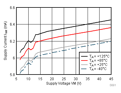
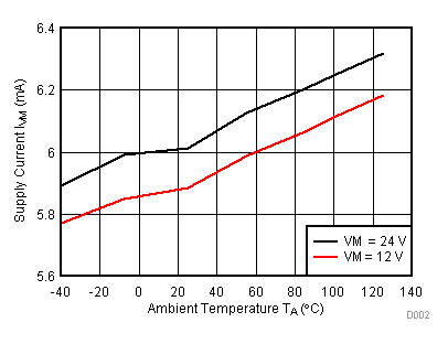
| IVM | VM operating supply current | nSLEEP high; ENABLE high; no motor load; VM = 24 V | 8 | 18 | mA | |
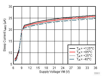
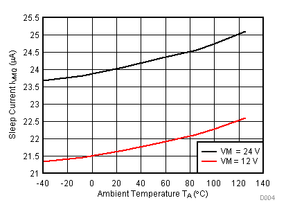
| IVMQ | VM sleep mode supply current | nSLEEP low; VM = 24 V; TA = 25°C | 28 | μA | ||
| nSLEEP low; VM = 24 V; TA = 125°C (1) | 77 | |||||
| tSLEEP | Sleep time | nSLEEP low to sleep mode | 100 | μs | ||
| tWAKE | Wake-up time | nSLEEP high to output transition | 1.5 | ms | ||
| tON | Turn-on time | VM > VUVLO2 to output transition | 1.5 | ms | ||
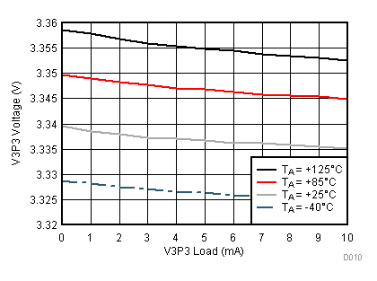
| V3P3 | LDO regulator voltage | External load 0 to 10 mA | 2.9 | 3.3 | 3.6 | V |
| CHARGE PUMP (VCP, CPH, CPL) | ||||||
| VCP | VCP operating voltage | VM > 12 V | VM + 11.5 | V | ||
| VUVLO2 < VM < 12 V | 2×VM – 1.5 | |||||
| ƒVCP (1) | Charge pump switching frequency | VM > VUVLO2 | 175 | 715 | kHz | |
| LOGIC-LEVEL INPUTS (STEP, DIR, ENABLE, nSLEEP, TRQ0, TRQ1, ATE) | ||||||
| VIL | Input logic low voltage | 0 | 0.6 | V | ||
| VIH | Input logic high voltage | 1.6 | 5.3 | V | ||
| VHYS | Input logic hysteresis | 100 | mV | |||
| IIL | Input logic low current | VIN = 0 V | –1 | 1 | μA | |
| IIH | Input logic high current | VIN = 5.0 V | 50 | 100 | μA | |
| RPD | Pulldown resistance | Measured between the pin and GND | 100 | kΩ | ||
| tPD | Propagation delay | STEP input to current change | 450 | ns | ||
| TRI-LEVEL INPUTS (M0, M1, DECAY0, DECAY1, TOFF) | ||||||
| VIL | Tri-level input logic low voltage | 0 | 0.6 | V | ||
| VIZ | Tri-level input Hi-Z voltage | 1.1 | V | |||
| VIH | Tri-level input logic high voltage | 1.6 | 5.3 | V | ||
| VHYS | Tri-level input hysteresis | 100 | mV | |||
| IIL | Tri-level input logic low current | VIN = 0 V | –55 | –35 | μA | |
| IIZ | Tri-level input Hi-Z current | VIN = 1.3 V | 15 | μA | ||
| IIH | Tri-level input logic high current | VIN = 3.3 V | 85 | μA | ||
| RPD | Tri-level pulldown resistance | Measured between the pin and GND | 40 | kΩ | ||
| RPU | Tri-level pullup resistance | Measured between V3P3 and the pin | 45 | kΩ | ||
| CONTROL OUTPUTS (nFAULT) | ||||||
| VOL | Output logic low voltage | IO = 4 mA | 0.5 | V | ||
| IOH | Output logic high leakage | External pullup resistor to 3.3 V | –1 | 1 | μA | |
| MOTOR DRIVER OUTPUTS (AOUT1, AOUT2, BOUT1, BOUT2) | ||||||
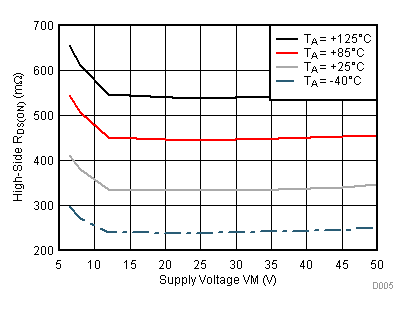
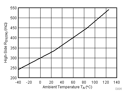
| RDS(ON) | High-side FET on resistance | VM = 24 V, I = 1 A, TA = 25°C | 330 | mΩ | ||
| VM = 24 V, I = 1 A, TA = 125°C (1) | 400 | 440 | ||||
| VM = 6.5 V, I = 1 A, TA = 25°C | 430 | |||||
| VM = 6.5 V, I = 1 A, TA = 125°C (1) | 500 | 560 | ||||
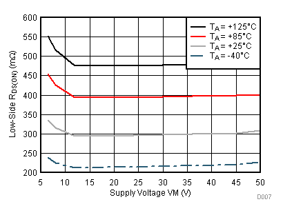
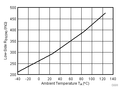
| RDS(ON) | Low-side FET on resistance | VM = 24 V, I = 1 A, TA = 25°C | 300 | mΩ | ||
| VM = 24 V, I = 1 A, TA = 125°C (1) | 370 | 400 | ||||
| VM = 6.5 V, I = 1 A, TA = 25°C | 370 | |||||
| VM = 6.5 V, I = 1 A, TA = 125°C (1) | 450 | 490 | ||||
| tRISE | Output rise time | VM = 24 V, 50 Ω load from xOUTx to GND | 70 | ns | ||
| tFALL | Output fall time | VM = 24 V, 50 Ω load from VM to xOUTx | 70 | ns | ||
| tDEAD | Output dead time (2) | 200 | ns | |||
| Vd | Body diode forward voltage | IOUT = 0.5 A | 0.7 | 1 | V | |
| PWM CURRENT CONTROL (VREF, AISEN, BISEN) | ||||||
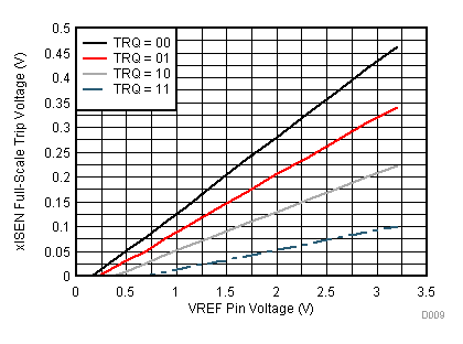
| VTRIP | xISENSE trip voltage, full scale | TRQ at 100%, VREF = 3.3 V | 500 | mV | ||
| TRQ at 75%, VREF = 3.3 V | 375 | |||||
| TRQ at 50%, VREF = 3.3 V | 250 | |||||
| TRQ at 25%, VREF = 3.3 V | 125 | |||||
| AV | Amplifier attenuation | TRQ at 100% (TRQ0 = 0, TRQ1 = 0) | 6.25 | 6.58 | 6.91 | V/V |
| TRQ at 75% (TRQ0 = 1, TRQ1 = 0) | 6.2 | 6.56 | 6.92 | |||
| TRQ at 50% (TRQ0 = 0, TRQ1 = 1) | 6.09 | 6.51 | 6.94 | |||
| TRQ at 25% (TRQ0 = 1, TRQ1 = 1) | 5.83 | 6.38 | 6.93 | |||
| tOFF | PWM off-time | TOFF Logic Low | 20 | μs | ||
| TOFF Logic High | 30 | |||||
| TOFF Hi-Z | 10 | |||||
| tBLANK | PWM blanking time | See Table 9 for details | 1.8 | µs | ||
| 1.5 | ||||||
| 1.2 | ||||||
| 0.9 | ||||||
| PROTECTION CIRCUITS | ||||||
| VUVLO2 | VM undervoltage lockout | VM falling; UVLO2 report | 5.8 | 6.4 | V | |
| VM rising; UVLO2 recovery | 6.1 | 6.5 | ||||
| VUVLO1 | Logic undervoltage | VM falling; logic disabled | 4.5 | 4.9 | V | |
| VM rising; logic enabled | 4.8 | 5 | ||||
| VUVLO,HYS | undervoltage hysteresis | Rising to falling threshold | 100 | mV | ||
| VCPUV | Charge pump undervoltage | VCP falling; CPUV report | VM + 1.8 | V | ||
| VCP rising; CPUV recovery | VM + 1.9 | |||||
| VCPUV,HYS | CP undervoltage hysteresis | Rising to falling threshold | 50 | mV | ||
| IOCP | Overcurrent protection trip level | Current through any FET | 2.5 | 3.6 | A | |
| VOCP | Sense pin overcurrent trip level | Voltage at AISEN or BISEN | 0.9 | 1.25 | V | |
| tOCP | Overcurrent deglitch time | 2 | μs | |||
| tRETRY | Overcurrent retry time | 0.5 | 2 | ms | ||
| TTSD (2) | Thermal shutdown temperature | Die temperature TJ | 150 | °C | ||
| THYS (2) | Thermal shutdown hysteresis | Die temperature TJ | 35 | °C | ||
(1) Specified by design and characterization data
(2) Specified by design and characterization data
6.6 Indexer Timing Requirements
| NO. | MIN | MAX | UNIT | ||
|---|---|---|---|---|---|
| 1 | ƒSTEP | Step frequency | 1 (1) | MHz | |
| 2 | tWH(STEP) | Pulse duration, STEP high | 470 | ns | |
| 3 | tWL(STEP) | Pulse duration, STEP low | 470 | ns | |
| 4 | tSU(DIR, Mx) | Setup time, DIR or Mx to STEP rising | 200 | ns | |
| 5 | tH(DIR, Mx) | Hold time, DIR or Mx to STEP rising | 200 | ns | |
(1) STEP input can operate up to 1 MHz, but system bandwidth is limited by the motor load
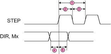 Figure 1. Timing Diagram
6.7 Typical Characteristics
Over recommended operating conditions (unless otherwise noted)