ZHCSBM8C September 2013 – October 2014 DRV8860
PRODUCTION DATA.
- 1 特性
- 2 应用范围
- 3 说明
- 4 简化电路原理图
- 5 修订历史记录
- 6 Pin Configuration and Functions
- 7 Specifications
- 8 Detailed Description
- 9 Application and Implementation
- 10Power Supply Recommendations
- 11Layout
- 12器件和文档支持
- 13机械封装和可订购信息
封装选项
机械数据 (封装 | 引脚)
散热焊盘机械数据 (封装 | 引脚)
- PWP|16
订购信息
8 Detailed Description
8.1 Overview
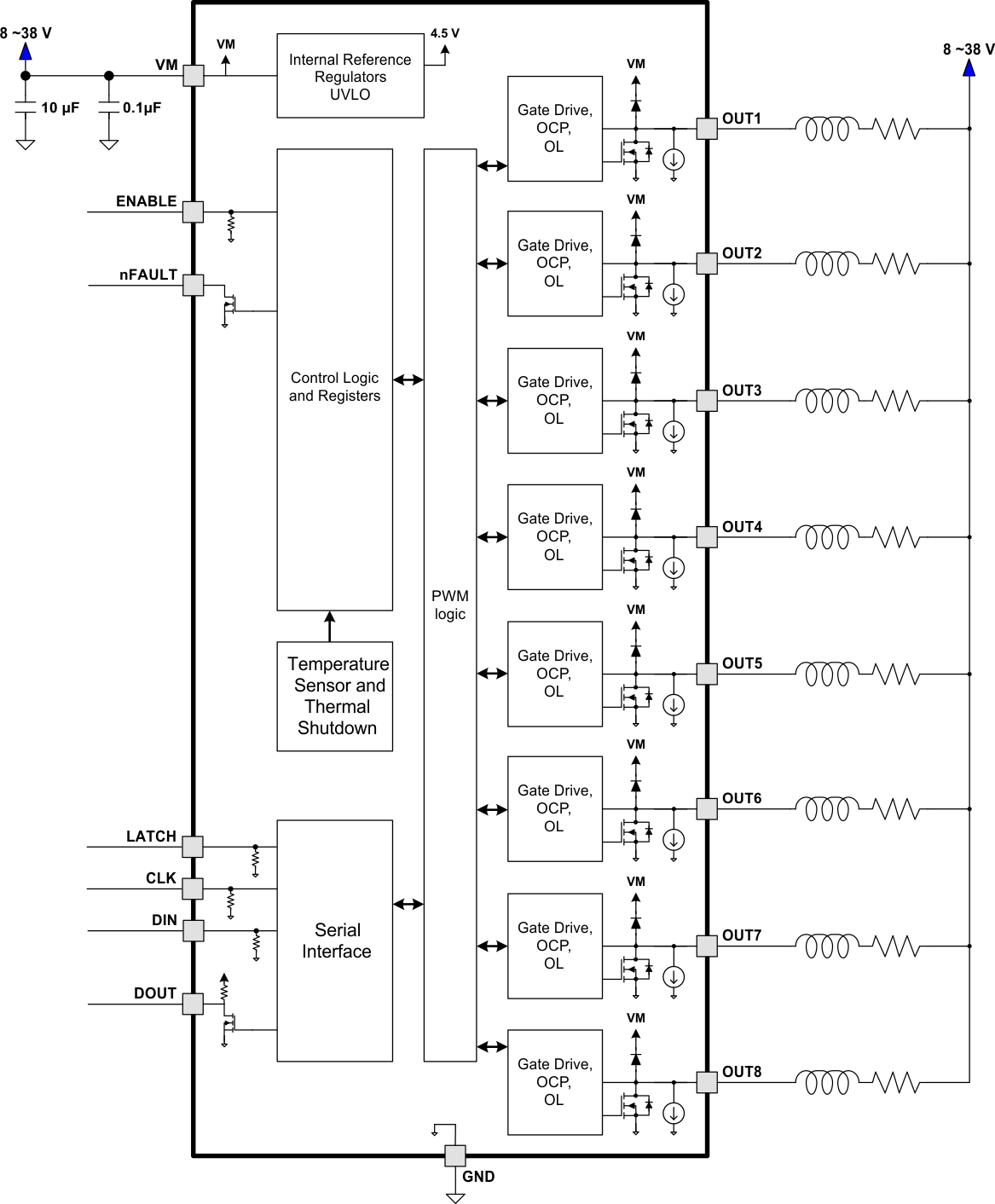
The DRV8860 is an integrated 8-channel low side driver with overcurrent protection and open/short detection. It has built-in diodes to clamp turn-off transients generated by inductive loads, and can be used to drive unipolar stepper motors, DC motors, relays, solenoids, or other loads.
DRV8860 can supply up to 200 mA x 8 channel continuous output current. The current driving capability increases with lower PWM duty cycle. A single channel can deliver up to 560 mA continuous output current. Refer to the current capability table for details.
A serial interface is provided to control the DRV8860 output drivers, configure internal register settings, and read the fault status of each channel. Multiple DRV8860 devices can be daisy-chained together to use a single serial interface. Energizing-time and holding-PWM-duty cycle are configurable through the serial interface as well. These functions allow for cooler running than traditional always-on solutions.
Internal shutdown functions are provided for overcurrent protection, short-circuit protection, unde voltage lockout and over temperature. DRV8860 can diagnosis an open load condition. Fault information for each channel can be read out through serial interface and is indicated by an external fault pin.
8.2 Functional Block Diagram
8.3 Feature Description
8.3.1 Recommended Output Current
DRV8860 current capability will depend on several system application parameters such as system ambient temperature, maximum case temperature, and overall output duty cycle. The PWP package provides a better heatsinking capability through the PowerPAD™; and therefore, is cable of driving higher output current or operating at a slightly lower temperature than the device in PW package.
| OUTPUT CURRENT RECOMMENDATION (PW PACKAGE) TA = 25°C | |
|---|---|
| CONFIGURATION | OUTPUT CURRENT CAPACITY |
| 1x output on (100% duty cycle) | 566 mA |
| 2x outputs on (100% duty cycle) | 400 mA per output |
| 4x outputs on (100% duty cycle) | 283 mA per output |
| 8x outputs on (100% duty cycle) | 200 mA per output |
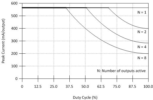 Figure 3. Output Current Capacity vs Duty Cycle for PW Package
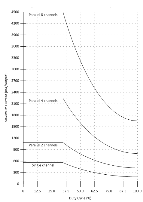 Figure 4. Maximum Current Capacity vs Duty Cycle when Paralleling Outputs for DRV8860PW
8.3.2 Daisy Chain Connection
Two or more DRV8860 devices may be connected together to use a single serial interface. The SDATOUT pin of the first device in the chain is connected to the SDATIN pin of the next device. The SCLK, LATCH, RESET, and nFAULT pins are connected together.
Timing diagrams are shown in Figure 5 and Figure 6 for the configuration of single devices, as well as two devices in daisy-chain connection.
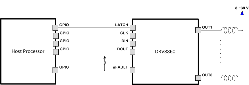 Figure 5. Single Device Connection
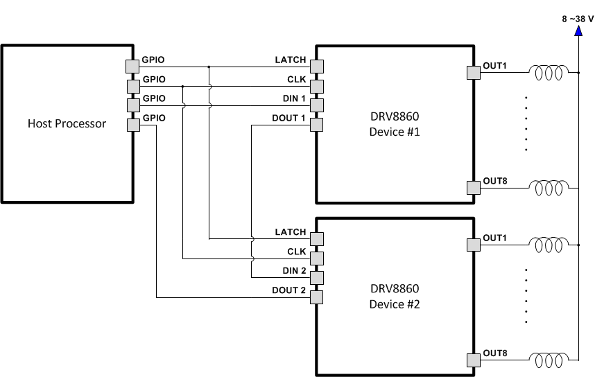 Figure 6. Daisy-Chain Connection
8.3.3 Protection Circuits
The DRV8860 is fully protected against undervoltage, overcurrent and overtemperature events.
8.3.3.1 Overcurrent Protection (OCP)
When output current exceeds OCP trigger level, corresponding channel will be automatically turned off. nFault pin will be set low and corresponding OCP flag in fault register will be set to 1.
Over current faults are automatically cleared whenever the corresponding output is turned off by setting the Data register bit to ‘0’. Alternatively, a Fault Reset special command will also clear this value. In either case, once all bits in the Fault register are clear, nFAULT is released.
8.3.3.2 Open Load Detection (OL)
When any output is in off status (the corresponding Data Register bit is set to ‘0’), a current sink pulls the node down with approximately 30 µA. If the voltage on the pin is sensed to be less than 1.2 V, then an open load condition is reported. nFAULT is driven low and the OL bit of the fault register (F8:F1) corresponding to the specific channel is set.
Open load faults are automatically cleared whenever the corresponding output is turned on by setting the Data register bit to ‘1’. Alternatively, a Fault Reset special command will also clear this value. In either case, once all bits in the Fault register are clear, nFAULT is released.
8.3.3.3 Thermal Shutdown (TSD)
If the die temperature exceeds safe limits, all outputs will be disabled, and the nFAULT pin will be driven low. Once the die temperature has fallen to a safe level, operation will automatically resume. The nFAULT pin will be released after operation has resumed.
8.3.3.4 Undervoltage Lockout (UVLO)
If at any time the voltage on the VM pin falls below the undervoltage lockout threshold voltage, all circuitry in the device will be disabled and internal logic will be reset. Operation will resume when VM rises above the UVLO threshold. nFAULT will not be asserted in this condition.
8.3.3.5 Digital Noise Filter
The DRV8860 features an internal noise filter on all digital inputs. In a noisy system, noise may disturb the serial daisy-chain interface. Without an input filter, this noise may result in an unexpected behavior or output state. The digital input filter is capable of removing unwanted noise frequencies while allowing fast communication over the serial interface.
8.4 Device Functional Modes
8.4.1 Internal Registers
The DRV8860 is controlled with a simple serial interface. There are three register banks that are used during operation: the Data register, the Control register, and the Fault register.
Register data movement flow and direction will be affected by special command.
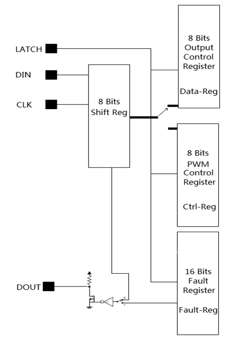 Figure 7. Register Data Movement
In default condition, 8 Bit shift register data moves into output control register DATA-REG.
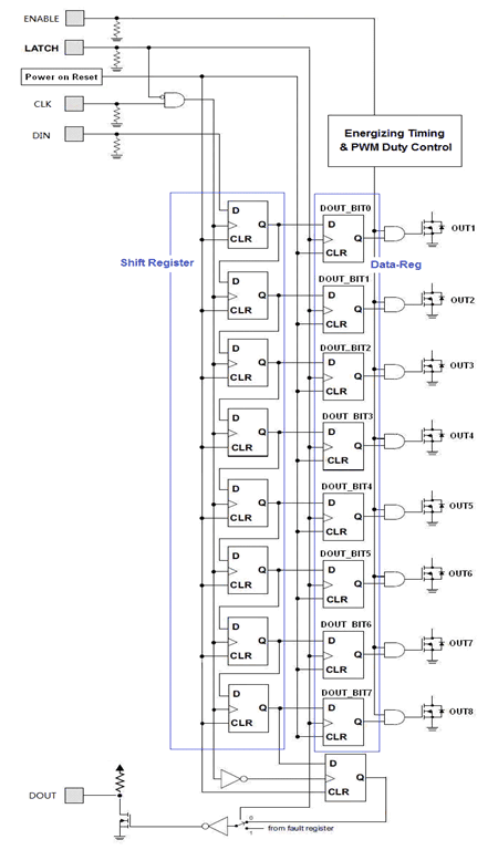 Figure 8. 8 Bit Shift Register Data Movement
8.5 Programming
8.5.1 Serial Control Interface
DRV8860 is using a daisy chain serial interface. Data is latched into the register on the rising edge of the LATCH pin. Data is clocked in on the rising edge of CLK when writing, and data is clocked out on the falling edge of CLK when reading.
8.5.1.1 Data Writing Waveform
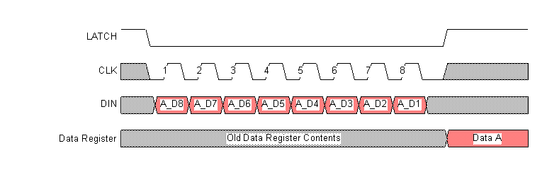 Figure 9. Writing Data Register – Single Device
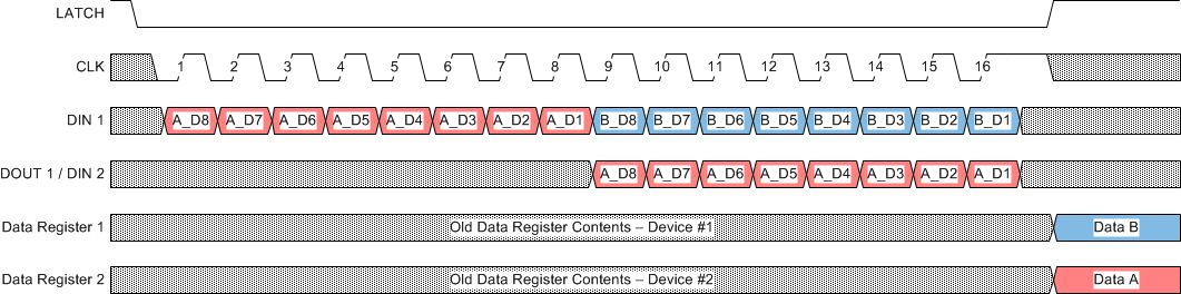 Figure 10. Writing Data Register – Daisy Chan
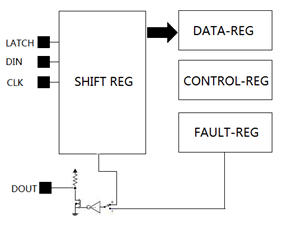 Figure 11. Writing Data Register – Data Flow
8.5.1.2 Fault Register Reading Waveform
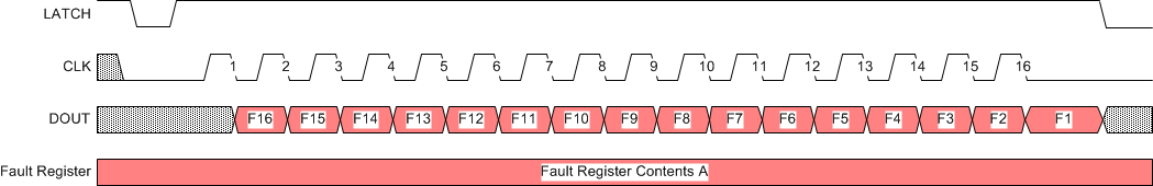 Figure 12. Reading Fault Register – Single Device
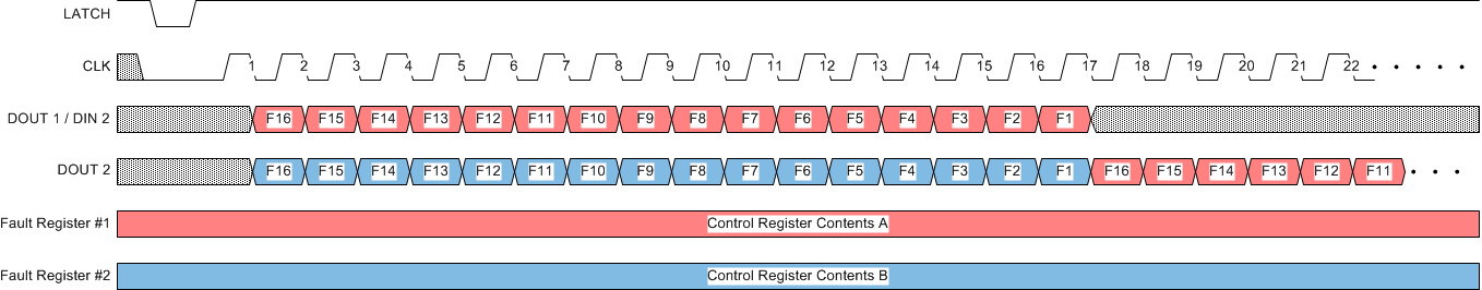 Figure 13. Reading Fault Register – Daisy Chain
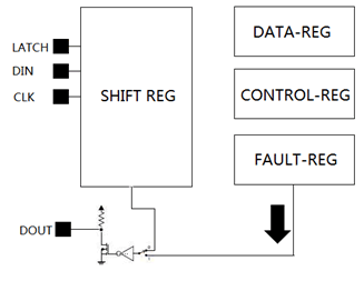 Figure 14. Reading Fault Register – Data Flow
8.5.1.3 Special Command
Besides output ON/OFF control and fault status reading back, DRV8860 has special functions to make system more robust or power efficient. These functions will need special command to initiate the device or configure the internal registers.
There are 5 Special Commands:
- Write Control Register command
- Read Control Register command
- Read Data Register command
- Fault Register Reset command
- PWM Start command
Special wave form pattern on CLK and LATCH pin will issue the special command, as below
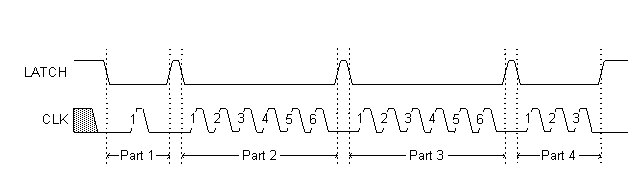 Figure 15. Special Command
| SPECIAL COMMAND | CLK CYCLES IN EACH PART | |||
|---|---|---|---|---|
| Part 1 | Part 2 | Part 3 | Part 4 | |
| Write Control Register | 1 | 2 | 2 | 3 |
| Read Control Register | 1 | 4 | 2 | 3 |
| Read Data Register | 1 | 4 | 4 | 3 |
| Fault Register Reset | 1 | 2 | 4 | 3 |
| PWM Start | 1 | 6 | 6 | 3 |
8.5.1.3.1 Special command: Write Control Register
When Write-Control-Register command is issued, the following serial data will be latched into timing and duty control register.
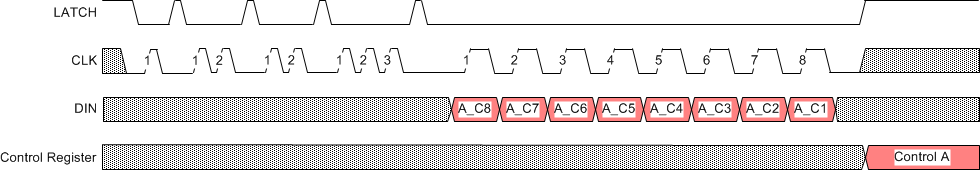 Figure 16. Writing Control Register – Single Device
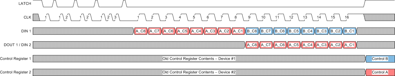 Figure 17. Writing Control Register – Daisy Chain
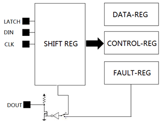 Figure 18. Writing Control Register – Data Flow
8.5.1.3.2 Special command: Read Control Register
When Read-Control-Register command is issued, control register content will be copied to internal shift register and following CLK will shift this content out from DOUT pin. This provides a mechanism for system to verify the control register is correctly programmed.
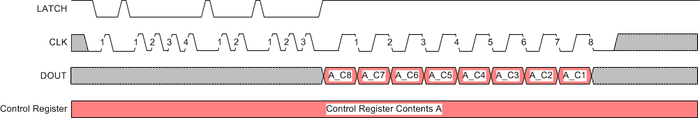 Figure 19. Read Control Register – Single Device
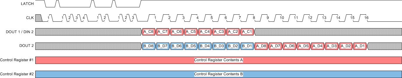 Figure 20. Read Control Register – Daisy Chain
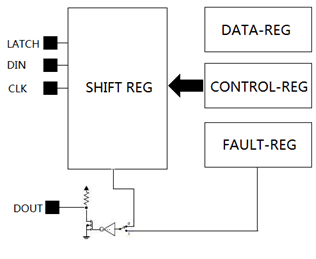 Figure 21. Read Control Register – Data Flow
8.5.1.3.3 Special command: Read Data Register
When Read-Data-Register command is issued, internal output data register content will be copied to internal shift register and following CLK will shift this content out from DOUT pin. This provides a mechanism for system to verify the output data is correctly programmed. It makes system more robust in noisy system.
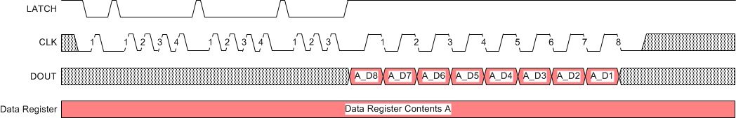 Figure 22. Reading Data Register – Single Device
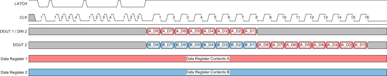 Figure 23. Reading Data Register – Daisy Chain
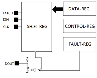 Figure 24. Reading Data Register – Data Flow
8.5.1.3.4 Special command: Fault Register Reset
When Fault-Register-Reset command is issued, internal 16bit fault register will be cleared. System can use this method to clear out all fault condition in every chained device at once.
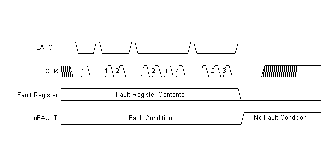 Figure 25. Fault Register Reset
8.5.1.3.5 Special command: PWM Start
When Fault-Register-Reset command is issued, output channel will ignore energizing time and directly enter into PWM mode following the setting in control register.
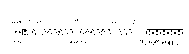 Figure 26. PWM Start Command
8.5.1.4 Output Energizing and PWM Control
The device output is defined by two stages: Energizing Phase and PWM Phase.
During the Energizing phase, the channel is turned on with 100% duty cycle for a duration set by Control register bits C4:C1.
In PWM chopping phase, with the PWM Duty Cycle defined by Control register bits C7:C5.
The behavior of each bit in the Control Register is described in Table 2.
Table 2. Control Register Settings
| C8 | C7 | C6 | C5 | C4 | C3 | C2 | C1 | Value | DESCRIPTION | |
|---|---|---|---|---|---|---|---|---|---|---|
| 0 | X | X | X | X | X | X | X | N/A | Outputs always in Energizing mode | |
| 1 | X | X | X | 0 | 0 | 0 | 0 | 0 ms | No Energizing, starts in PWM chopping | |
| 1 | X | X | X | 0 | 0 | 0 | 1 | 3 ms | Sets the Energizing Time (100% duty cycle) before switching to PWM Phase | |
| 1 | X | X | X | 0 | 0 | 1 | 0 | 5 ms | ||
| 1 | X | X | X | 0 | 0 | 1 | 1 | 10 ms | ||
| 1 | X | X | X | 0 | 1 | 0 | 0 | 15 ms | ||
| 1 | X | X | X | 0 | 1 | 0 | 1 | 20 ms | ||
| 1 | X | X | X | 0 | 1 | 1 | 0 | 30 ms | ||
| 1 | X | X | X | 0 | 1 | 1 | 1 | 50 ms | ||
| 1 | X | X | X | 1 | 0 | 0 | 0 | 80 ms | ||
| 1 | X | X | X | 1 | 0 | 0 | 1 | 110 ms | ||
| 1 | X | X | X | 1 | 0 | 1 | 0 | 140 ms | ||
| 1 | X | X | X | 1 | 0 | 1 | 1 | 170 ms | ||
| 1 | X | X | X | 1 | 1 | 0 | 0 | 200 ms | ||
| 1 | X | X | X | 1 | 1 | 0 | 1 | 230 ms | ||
| 1 | X | X | X | 1 | 1 | 1 | 0 | 260 ms | ||
| 1 | X | X | X | 1 | 1 | 1 | 1 | 300 ms | ||
| 1 | 0 | 0 | 0 | X | X | X | X | 0% | Output is off after Energizing Phase | |
| 1 | 0 | 0 | 1 | X | X | X | X | 12.50% | 12.5 kHz | Sets PWM chopping duty cycle. DC is the duty cycle that the low-side FET is on. |
| 1 | 0 | 1 | 0 | X | X | X | X | 25.00% | 25 kHz | |
| 1 | 0 | 1 | 1 | X | X | X | X | 37.50% | 50 kHz | |
| 1 | 1 | 0 | 0 | X | X | X | X | 50.00% | ||
| 1 | 1 | 0 | 1 | X | X | X | X | 62.50% | ||
| 1 | 1 | 1 | 0 | X | X | X | X | 75.00% | ||
| 1 | 1 | 1 | 1 | X | X | X | X | 87.50% | ||
There are five operation cases as described in Figure 27 through Figure 31.
The output is turned on with 100% duty cycle.
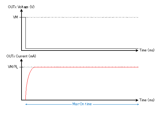 Figure 27. Case 1: Timer Enable Bit (C8) is 0 (Default Value)
The output is turned on in PWM chopping mode with duty cycle defined by Control register bits C7:C5.
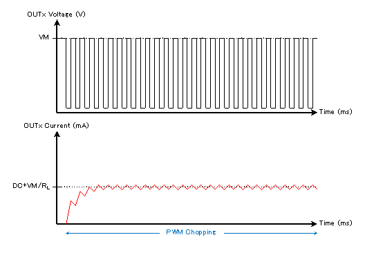 Figure 28. Case 2: Timer Enable Bit (C8) is 1 and Energizing Timing Bits (C4:C1) are 0000
The output is turned on in Energizing mode with 100% duty cycle for a duration set by Control register bits C4:C1. After the timer expires, the output switches to PWM chopping mode with PWM Duty Cycle defined by Control register bits C7:C5.
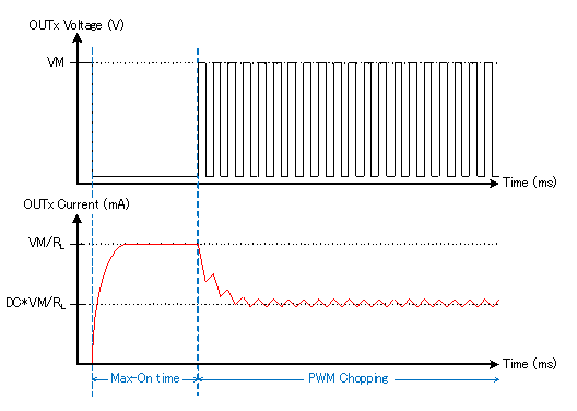 Figure 29. Case 3: Timer Enable Bit (C8) is 1, Energizing Timing Bits (C4:C1) are NOT 0000, and PWM Duty Bits (C7:C5) are NOT 000
The output is turned on in Energizing mode with 100% duty cycle for a duration set by Control register bits C4:C1. After the timer expires, the output is turned off.
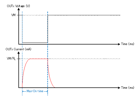 Figure 30. Case 4: Timer Enable Bit (C8) is 1, Energizing Timing Bits (C4:C1) are NOT 0000, and PWM Duty Bits (C7:C5) are 00
8.5.1.4.1 PWM Start Special Command Used
The output is turned on in Energizing mode with 100% duty cycle, and a timer is enabled with duration set by Control register bits C4:C1. If the PWM Start special command is received before the timer expires, then the output switches to PWM chopping mode with PWM Duty Cycle defined by Control register bits C7:C5. If the timer expires and no PWM Start is received, then the device will stay in Energizing mode regardless of other PWM Start commands.
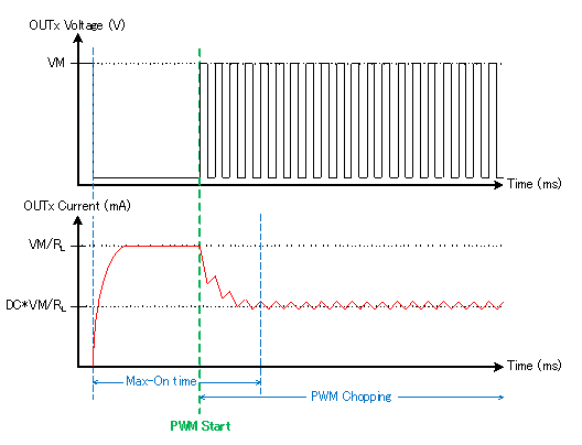 Figure 31. Case 5: Timer Enable Bit (C8) is 0, Energizing Timing Bits (C4:C1) are NOT 0000, and PWM Duty Bits (C7:C5) are NOT 000
8.6 Register Maps
8.6.1 Data Register
The Data register is used to control the status of each of the eight outputs:
| D8 | D7 | D6 | D5 | D4 | D3 | D2 | D1 |
| OUT8 | OUT7 | OUT6 | OUT5 | OUT4 | OUT3 | OUT2 | OUT1 |
| R/W | R/W | R/W | R/W | R/W | R/W | R/W | R/W |
| LEGEND: R/W = Read/Write; R = Read only; -n = value after reset |
When any bit is ‘1’, the corresponding output will be active. When any bit is ‘0’, the output will be inactive.
The data register is the default write location for the serial interface. In order to read back data from this register, the Data Register Readout special command is used.
8.6.2 Fault Register
The Fault register can be read to determine if any channel exist fault condition. OCP is an overcurrent fault and OLD is an open load fault.
| F16 | F15 | F14 | F13 | F12 | F11 | F10 | F9 |
| OUT8 OCP | OUT7 OCP | OUT6 OCP | OUT5 OCP | OUT4 OCP | OUT3 OCP | OUT2 OCP | OUT1 OCP |
| R/W | R/W | R/W | R/W | R/W | R/W | R/W | R/W |
| F8 | F7 | F6 | F5 | F4 | F3 | F2 | F1 |
| OUT8 OL | OUT7 OL | OUT6 OL | OUT5 OL | OUT4 OL | OUT3 OL | OUT2 OL | OUT1 OL |
| R/W | R/W | R/W | R/W | R/W | R/W | R/W | R/W |
| LEGEND: R/W = Read/Write; R = Read only; -n = value after reset |
When any fault occurs, nFAULT pin will be driven low and corresponding Fault register bit will be set up as ‘1’. OCP is a flag indicating overcurrent fault. ODP is a flag indicating open load fault.
Fault bits can be reset by two approaches:
- Special command ‘FAULT RESET’ clear all fault bits.
- Setting Data register to ON will clear corresponding OLD bits.
Setting Data register to OFF will clear corresponding OCP bits.
8.6.3 Control Register
The Control register is used to adjust the Energizing Time and PWM Duty Cycle of outputs:
| C8 | C7 | C6 | C5 | C4 | C3 | C2 | C1 |
| Over All Enable | PWM Duty Cycle control | Energizing Time control | |||||
| R/W | R/W | R/W | |||||
| LEGEND: R/W = Read/Write; R = Read only; -n = value after reset |
Special command ‘WRITE CONTROL REGISTER’ is used to program control register.
Special command ‘READ CONTROL REGISTER’ is used to read back control register content.