ZHCSBM8C September 2013 – October 2014 DRV8860
PRODUCTION DATA.
- 1 特性
- 2 应用范围
- 3 说明
- 4 简化电路原理图
- 5 修订历史记录
- 6 Pin Configuration and Functions
- 7 Specifications
- 8 Detailed Description
- 9 Application and Implementation
- 10Power Supply Recommendations
- 11Layout
- 12器件和文档支持
- 13机械封装和可订购信息
封装选项
机械数据 (封装 | 引脚)
散热焊盘机械数据 (封装 | 引脚)
- PWP|16
订购信息
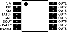
6 Pin Configuration and Functions
PW (TSSOP) PACKAGE
(TOP VIEW)
PWP (HTSSOP) PACKAGE
(TOP VIEW)
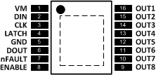
Pin Functions
| NAME | PIN | I/O(1) | DESCRIPTION | EXTERNAL COMPONENTS OR CONNECTIONS |
|---|---|---|---|---|
| GND | 5 | — | Device ground | All pins must be connected to ground |
| VM | 1 | — | Motor power supply | Connect to motor supply voltage. Bypass to GND with a 0.1 μF ceramic capacitor plus a 10 μF electrolytic capacitor. |
| ENABLE | 8 | I | Output stage enable control input | Logic high to enable outputs, logic low to disable outputs. Internal logic and registers can be read and written to when ENABLE is logic low. Internal pulldown. |
| LATCH | 4 | I | Serial latch signal | Refer to serial communication waveforms. Internal pulldown. |
| CLK | 3 | I | Serial clock input | Rising edge clocks data into part for write operations. Falling edge clocks data out of part for read operations. Internal pulldown. |
| DIN | 2 | I | Serial data input | Serial data input from controller. Internal pulldown. |
| DOUT | 6 | O | Serial data output | Serial data output to controller. Open-drain output with internal pullup. |
| nFAULT | 7 | OD | Fault | Logic low when in fault condition. Open-drain output requires external pullup. Faults: OCP, OL, OTS, UVLO |
| OUT1 | 16 | O | Low-side output 1 | NFET output driver. Connect external load between this pin and VM |
| OUT2 | 15 | O | Low-side output 2 | NFET output driver. Connect external load between this pin and VM |
| OUT3 | 14 | O | Low-side output 3 | NFET output driver. Connect external load between this pin and VM |
| OUT4 | 13 | O | Low-side output 4 | NFET output driver. Connect external load between this pin and VM |
| OUT5 | 12 | O | Low-side output 5 | NFET output driver. Connect external load between this pin and VM |
| OUT6 | 11 | O | Low-side output 6 | NFET output driver. Connect external load between this pin and VM |
| OUT7 | 10 | O | Low-side output 7 | NFET output driver. Connect external load between this pin and VM |
| OUT8 | 9 | O | Low-side output 8 | NFET output driver. Connect external load between this pin and VM |
(1) Directions: I = input, O = output, OD = open-drain output
Table 1. External Components
| COMPONENT | PIN 1 | PIN 2 | RECOMMENDED |
|---|---|---|---|
| C(VM1) | VM | GND | 0.1 µF ceramic capacitor rated for VM |
| 10 µF electrolytic capacitor rated for VM | |||
| R(nFAULT) | V3P3(1) | nFAULT | > 4.7 kΩ |
(1) V3P3 is not a pin on the DRV8860, but a V3P3 supply voltage pullup is required for open-drain output nFAULT.