ZHCSBM8C September   2013  – October 2014 DRV8860

PRODUCTION DATA.  

  1. 特性
  2. 应用范围
  3. 说明
  4. 简化电路原理图
  5. 修订历史记录
  6. Pin Configuration and Functions
  7. Specifications
    1. 7.1 Absolute Maximum Ratings
    2. 7.2 Handling Ratings
    3. 7.3 Recommended Operating Conditions
    4. 7.4 Thermal Information
    5. 7.5 Electrical Characteristics
    6. 7.6 Timing Requirements
    7. 7.7 Typical Characteristics
  8. Detailed Description
    1. 8.1 Overview
    2. 8.2 Functional Block Diagram
    3. 8.3 Feature Description
      1. 8.3.1 Recommended Output Current
      2. 8.3.2 Daisy Chain Connection
      3. 8.3.3 Protection Circuits
        1. 8.3.3.1 Overcurrent Protection (OCP)
        2. 8.3.3.2 Open Load Detection (OL)
        3. 8.3.3.3 Thermal Shutdown (TSD)
        4. 8.3.3.4 Undervoltage Lockout (UVLO)
        5. 8.3.3.5 Digital Noise Filter
    4. 8.4 Device Functional Modes
      1. 8.4.1 Internal Registers
    5. 8.5 Programming
      1. 8.5.1 Serial Control Interface
        1. 8.5.1.1 Data Writing Waveform
        2. 8.5.1.2 Fault Register Reading Waveform
        3. 8.5.1.3 Special Command
          1. 8.5.1.3.1 Special command: Write Control Register
          2. 8.5.1.3.2 Special command: Read Control Register
          3. 8.5.1.3.3 Special command: Read Data Register
          4. 8.5.1.3.4 Special command: Fault Register Reset
          5. 8.5.1.3.5 Special command: PWM Start
        4. 8.5.1.4 Output Energizing and PWM Control
          1. 8.5.1.4.1 PWM Start Special Command Used
    6. 8.6 Register Maps
      1. 8.6.1 Data Register
      2. 8.6.2 Fault Register
      3. 8.6.3 Control Register
  9. Application and Implementation
    1. 9.1 Application Information
    2. 9.2 Typical Application
      1. 9.2.1 Design Requirements
      2. 9.2.2 Detailed Design Procedure
        1. 9.2.2.1 Drive Current
      3. 9.2.3 Application Curves
  10. 10Power Supply Recommendations
    1. 10.1 Power Supply and Logic Sequencing
  11. 11Layout
    1. 11.1 Layout Guidelines
    2. 11.2 Layout Example
    3. 11.3 Thermal Consideration
      1. 11.3.1 Power Dissipation
      2. 11.3.2 Heatsinking
  12. 12器件和文档支持
    1. 12.1 商标
    2. 12.2 静电放电警告
    3. 12.3 术语表
  13. 13机械封装和可订购信息

封装选项

机械数据 (封装 | 引脚)
散热焊盘机械数据 (封装 | 引脚)
订购信息

10 Power Supply Recommendations

The DRV8860 is designed to operate from an input voltage supply (VM) range between 8 and 38 V. A 0.1-µF ceramic capacitor rated for VM must be placed as close as possible to the VM pin. In addition to the local decoupling cap, additional bulk capacitance is required and must be sized accordingly to the application requirements.

Bulk capacitance sizing is an important factor in motor drive system design. It is dependent on a variety of factors including:

  • Type of power supply
  • Acceptable supply voltage ripple
  • Parasitic inductance in the power supply wiring
  • Type of load
  • Load startup current

The inductance between the power supply and motor drive system will limit the rate current can change from the power supply. If the local bulk capacitance is too small, the system will respond to excessive current demands or dumps from the motor with a change in voltage. The user should size the bulk capacitance to meet acceptable voltage ripple levels.

The datasheet generally provides a recommended value but system level testing is required to determine the appropriate sized bulk capacitor.

Power_supply_example_slrs065.gif
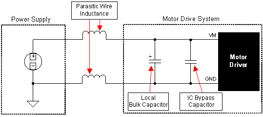
Figure 36. Example Setup of Motor Drive System with External Power Supply

10.1 Power Supply and Logic Sequencing

There is no specific sequence for powering-up the DRV8860. It is okay for digital input signals to be present before VM is applied. After VM is applied to the DRV8860, it begins operation based on the status of the control pins.