ZHCSB92G June 2013 – May 2017 DRV8711
PRODUCTION DATA.
- 1 特性
- 2 应用
- 3 说明
- 4 修订历史记录
- 5 Pin Configuration and Functions
- 6 Specifications
-
7 Detailed Description
- 7.1 Overview
- 7.2 Functional Block Diagram
- 7.3 Feature Description
- 7.4 Device Functional Modes
- 7.5 Programming
- 7.6
Register Maps
- 7.6.1 Control Registers
- 7.6.2 CTRL Register (Address = 0x00)
- 7.6.3 TORQUE Register (Address = 0x01)
- 7.6.4 OFF Register (Address = 0x02)
- 7.6.5 BLANK Register (Address = 0x03)
- 7.6.6 DECAY Register (Address = 0x04)
- 7.6.7 STALL Register (Address = 0x05)
- 7.6.8 DRIVE Register (Address = 0x06)
- 7.6.9 STATUS Register (Address = 0x07)
- 8 Application and Implementation
- 9 Power Supply Recommendations
- 10Layout
- 11器件和文档支持
- 12机械、封装和可订购信息
7 Detailed Description
7.1 Overview
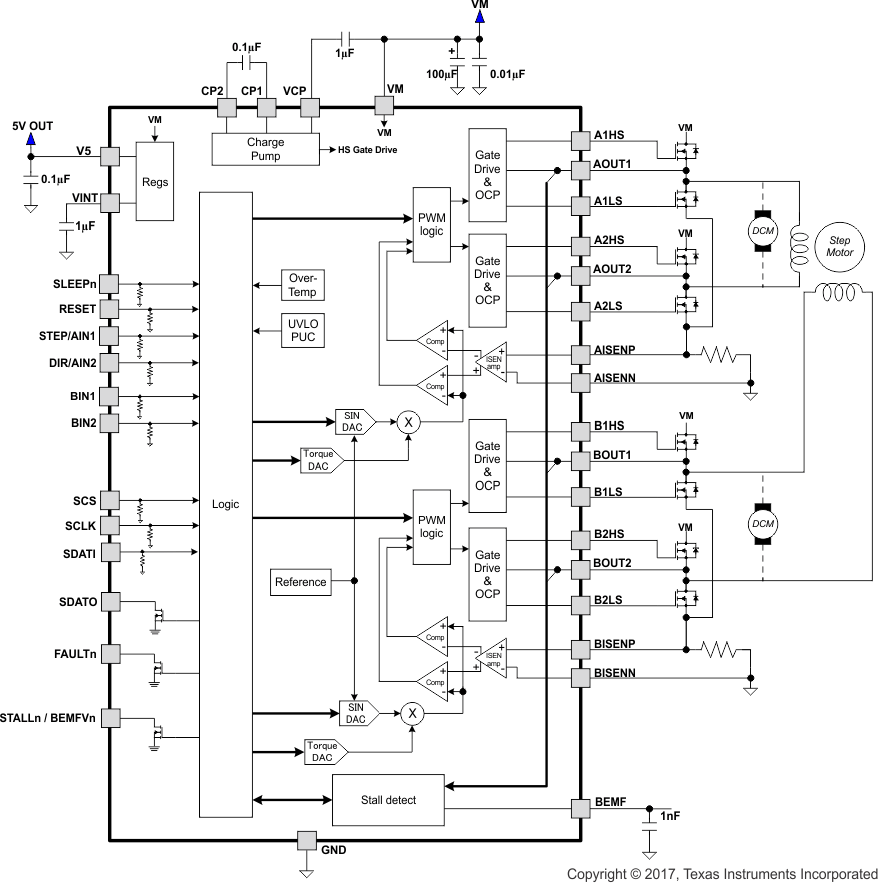
The DRV8711 device is a stepper motor controller that uses external N-channel MOSFETs to drive a bipolar stepper motor or two brushed DC motors. A microstepping indexer is integrated, which is capable of step modes from full step to 1/256-step.
An ultra-smooth motion profile can be achieved using adaptive blanking time, adjustable decay times, and various current decay modes, including an auto-mixed decay mode. When microstepping, motor stall can be reported with an optional back-EMF output.
A simple step/direction or PWM interface allows easy interfacing to controller circuits. A SPI serial interface is used to program the device operation. Output current (torque), step mode, decay mode, and stall detection functions are all programmable through a SPI serial interface.
Internal shutdown functions are provided for overcurrent protection, short-circuit protection, undervoltage lockout, and overtemperature. Fault conditions are indicated through a FAULTn pin, and each fault condition is reported through a dedicated bit through SPI.
7.2 Functional Block Diagram
7.3 Feature Description
Table 1 lists the critical components for the device.
Table 1. Critical Components
| PIN | NAME | COMPONENT |
|---|---|---|
| 4 | VM | 100-µF electrolytic rated for VM voltage to GND 0.01-µF ceramic rated for VM voltage to GND |
| 3 | VCP | 1-µF ceramic X7R rated 16 V to VCP |
| 1, 2 | CP1, CP2 | 0.1-µF rated for VM + 12 V between these pins |
| 6 | V5 | 0.1-µF ceramic X7R rated 6.3 V to GND |
| 7 | VINT | 1-µF ceramic X7R rated 6.3 V to GND |
| 17 | SDATO | Requires external pullup to logic supply |
| 18 | FAULTn | Requires external pullup to logic supply |
| 19 | STALLn/BEMFVn | Requires external pullup to logic supply |
| 20 | BEMF | 1-nF low-leakage capacitor to GND |
7.3.1 PWM Motor Drivers
The DRV8711 contains two H-bridge motor predrivers with current control PWM circuitry. More detailed descriptions of the subblocks are described in the following sections.
7.3.2 Direct PWM Input Mode
Direct PWM mode is selected by setting the PWMMODE bit in the OFF register. In direct PWM input mode, the AIN1, AIN2, BIN1, and BIN2 directly control the state of the output drivers. This allows for driving up to two brushed DC motors. The logic is shown in Table 2:
Table 2. Direct PWM Input Mode Logic
| xIN1 | xIN2 | xOUT1 | xOUT2 | OPERATION |
|---|---|---|---|---|
| 0 | 0 | Z | Z | Asynchronous Fast Decay |
| 0 | 1 | L | H | Reverse Drive |
| 1 | 0 | H | L | Forward Drive |
| 1 | 1 | L | L | Slow Decay |
If mixed or auto-mixed decay modes are used, they will apply to every cycle, because current change information is not available.
In direct PWM mode, the current control circuitry is still active. The full-scale VREF is set to 2.75 V. The TORQUE register may be used to scale this value, and the ISEN sense amp gain may still be set using the ISGAIN bits of the CTRL register.
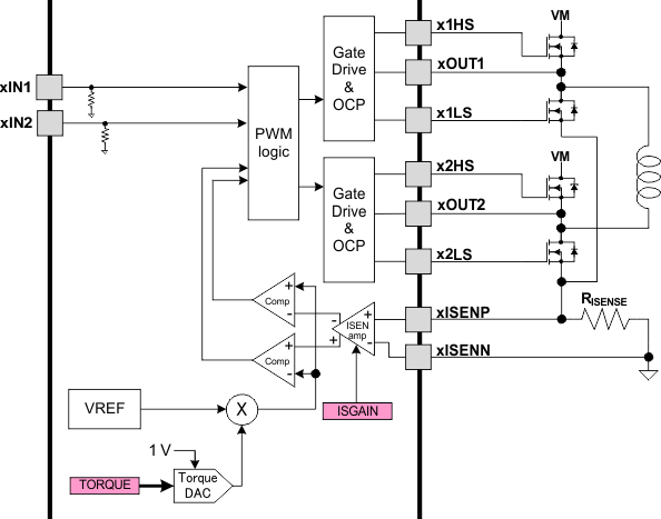 Figure 7. Direct PWM Input Mode
The current through the motor windings is regulated by an adjustable fixed-off-time PWM current regulation circuit. When an H-bridge is enabled, current rises through the winding at a rate dependent on the DC voltage and inductance of the winding and the magnitude of the back EMF present. Once the current hits the current chopping threshold, the bridge disables the current for a fixed period of time, which is programmable between 500 ns and 128 µs by writing to the TOFF bits in the OFF register. After the off time expires, the bridge is re-enabled, starting another PWM cycle.
The chopping current is set by a comparator which compares the voltage across a current sense resistor connected to the xISENx pins, multiplied by the gain of the current sense amplifier, with a reference voltage. The current sense amplifier is programmable in the CTRL register. When driving in PWM mode, the chopping current is calculated as follows:

Where TORQUE is the setting of the TORQUE bits, and ISGAIN is the programmed gain of the ISENSE amplifiers (5, 10, 20, or 40).
7.3.3 Microstepping Indexer
Built-in indexer logic in the DRV8711 allows a number of different stepping configurations. The MODE bits in the CTRL register are used to configure the stepping format as shown in Table 3.
Table 3. Microstepping Indexer Logic
| MODE3 | MODE2 | MODE1 | MODE0 | STEP MODE |
|---|---|---|---|---|
| 0 | 0 | 0 | 0 | Full-step (2-phase excitation) with 71% current |
| 0 | 0 | 0 | 1 | 1/2 step |
| 0 | 0 | 1 | 0 | 1/4 step |
| 0 | 0 | 1 | 1 | 1/8 step |
| 0 | 1 | 0 | 0 | 1/16 step |
| 0 | 1 | 0 | 1 | 1/32 step |
| 0 | 1 | 1 | 0 | 1/64 step |
| 0 | 1 | 1 | 1 | 1/128 step |
| 1 | 0 | 0 | 0 | 1/256 step |
Table 4 shows the relative current and step directions for full-step through 1/8-step operation. Higher microstepping resolutions follow the same pattern. The AOUT current is the sine of the electrical angle; BOUT current is the cosine of the electrical angle.
The reset state is 45°. This state is entered at power up or application of RESETn. This is shown in Table 4 by cells shaded in yellow.
Table 4. Step Directions
| FULL STEP | 1/2 STEP | 1/4 STEP | 1/8 STEP | AOUT CURRENT (% FULL-SCALE) |
BOUT CURRENT (% FULL-SCALE) |
ELECTRICAL ANGLE (DEGREES) |
|---|---|---|---|---|---|---|
| 1 | 1 | 1 | 0 | 100 | 0 | |
| 2 | 20 | 98 | 11.325 | |||
| 2 | 3 | 38 | 92 | 22.5 | ||
| 4 | 56 | 83 | 33.75 | |||
| 1 | 2 | 3 | 5 | 71 | 71 | 45 (home state) |
| 6 | 83 | 56 | 56.25 | |||
| 4 | 7 | 92 | 38 | 67.5 | ||
| 8 | 98 | 20 | 78.75 | |||
| 3 | 5 | 9 | 100 | 0 | 90 | |
| 10 | 98 | –20 | 101.25 | |||
| 6 | 11 | 92 | –38 | 112.5 | ||
| 12 | 83 | –56 | 123.75 | |||
| 2 | 4 | 7 | 13 | 71 | –71 | 135 |
| 14 | 56 | –83 | 146.25 | |||
| 8 | 15 | 38 | –92 | 157.5 | ||
| 16 | 20 | –98 | 168.75 | |||
| 5 | 9 | 17 | 0 | –100 | 180 | |
| 18 | –20 | –98 | 191.25 | |||
| 10 | 19 | –38 | –92 | 202.5 | ||
| 20 | –56 | –83 | 213.75 | |||
| 3 | 6 | 11 | 21 | –71 | –71 | 225 |
| 22 | –83 | –56 | 236.25 | |||
| 12 | 23 | –92 | –38 | 247.5 | ||
| 24 | –98 | –20 | 258.75 | |||
| 7 | 13 | 25 | –100 | 0 | 270 | |
| 26 | –98 | 20 | 281.25 | |||
| 14 | 27 | –92 | 38 | 292.5 | ||
| 28 | –83 | 56 | 303.75 | |||
| 4 | 8 | 15 | 29 | –71 | 71 | 315 |
| 30 | –56 | 83 | 326.25 | |||
| 16 | 31 | –38 | 92 | 337.5 | ||
| 32 | –20 | 98 | 348.75 |
At each rising edge of the STEP input, or each time a 1 is written to the RSTEP bit in the CTRL register, the indexer travels to the next state in the table. The direction is shown with the DIR pin high and the RDIR bit in the CTRL register set to 0, or the DIR pin low and the RDIR bit set to 1. If the DIR pin is low with the RDIR bit 0, or the DIR pin is high with the RDIR bit 1, the sequence is reversed. Positive current is defined as xOUT1 = positive with respect to xOUT2.
If the step mode is changed while stepping, the indexer will advance to the next valid state for the new MODE setting at the rising edge of STEP.
7.3.4 Current Regulation
The current through the motor windings is regulated by an adjustable fixed-off-time PWM current regulation circuit. When an H-bridge is enabled, current rises through the winding at a rate dependent on the DC voltage and inductance of the winding and the magnitude of the back EMF present. Once the current hits the current chopping threshold, the bridge disables the current for a fixed period of time, which is programmable between 500 nS and 128 µS by writing to the TOFF bits in the OFF register. After the off time expires, the bridge is re-enabled, starting another PWM cycle.
In stepping motors, current regulation is used to vary the current in the two windings in a sinusoidal fashion to provide smooth motion.
The PWM chopping current is set by a comparator which compares the voltage across a current sense resistor connected to the xISENx pins, multiplied by the gain of the current sense amplifier, with a reference voltage. The current sense amplifier is programmable in the CTRL register.
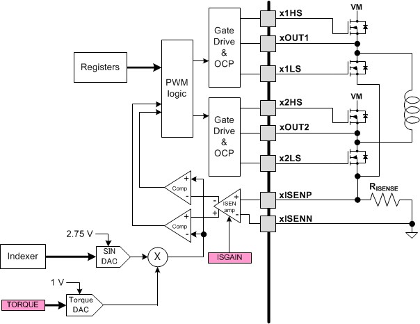 Figure 8. PWM Chopping Current
To generate the reference voltage for the current chopping comparator, the output of a sine lookup table is multiplied by the value of the bits in the TORQUE register. This result is applied to a sine-weighted DAC, whose full-scale output voltage is 2.75 V.
Therefore, the full-scale (100%) chopping current is calculated as follows:

where
- TORQUE is the setting of the TORQUE bits
- ISGAIN is the programmed gain of the ISENSE amplifiers (5, 10, 20, or 40)
Example:
If a 0.1-Ω sense resistor is used, ISGAIN is set to 0 (gain of 5), and TORQUE is set to 255, the full-scale (100%) chopping current will be (2.75 V * 255) / (256 * 5 * 0.1 Ω) = 5.5 A.
7.3.5 Decay Modes
During PWM current chopping, the H-bridge is enabled to drive through the motor winding until the PWM current chopping threshold is reached. This is shown in Figure 9, Item 1. The current flow direction shown indicates positive current flow in the step table below.
Once the chopping current threshold is reached, the H-bridge can operate in two different states, fast decay or slow decay.
In fast decay mode, once the PWM chopping current level has been reached, the H-bridge reverses state to allow winding current to flow in a reverse direction. The opposite FETs are turned on; as the winding current approaches zero, the bridge is disabled to prevent any reverse current flow. Fast decay mode is shown in Figure 9, item 2.
In slow decay mode, winding current is recirculated by enabling both of the low-side FETs in the bridge. This is shown in Figure 9, Item 3.
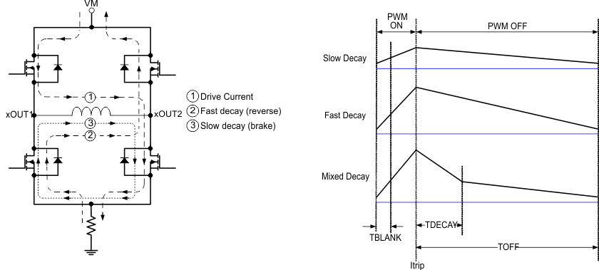 Figure 9. Decay Modes
The DRV8711 supports fast decay and slow decay modes in both indexer and direct PWM modes. In addition, in indexer mode only, it supports fixed mixed decay and auto-mixed decay modes. Decay mode is selected by the DECMOD bits in the DECAY register.
Mixed decay mode begins as fast decay, but after a programmable period of time (set by the TDECAY bits in the DECAY register) switches to slow decay mode for the remainder of the fixed off time. Even if mixed decay is selected, if the current is increasing or remaining the same (per the step table), then slow decay is used.
Auto-mixed decay mode samples the current level at the end of the blanking time, and if the current is above the Itrip threshold, immediately changes the H-bridge to fast decay. During fast decay, the (negative) current is monitored, and when it falls below the Itrip threshold (and another blanking time has passed), the bridge is switched to slow decay. Once the fixed off time expires, a new cycle is started.
If the bridge is turned on and at the end of TBLANK the current is below the Itrip threshold, the bridge remains on until the current reaches Itrip. Then slow decay is entered for the fixed off time, and a new cycle begins.
The upper waveform shows the behavior if I < Itrip at the end of tBLANK. At slow motor speeds, where back EMF is not significant, the current increase during the ON phase is the same magnitude as the current decrease in fast decay, because both times are controlled by tBLANK, and the rate of change is the same (full VM is applied to the load inductance in both cases, but in opposite directions). In this case, the current will gradually be driven down until the peak current is just hitting Itrip at the end of the blanking time, after which some cycles will be slow decay, and some will be mixed decay.
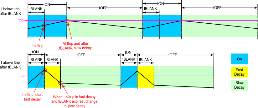 Figure 10. I < Itrip at the End of tBLANK
If the Itrip level changes during a PWM cycle (in response to a step command to the indexer), the current cycle is immediately terminated, and a new cycle is begun. Refer to the drawing below.
If the Itrip level has increased, the H-bridge will immediately turn on; if the Itrip level has decreased, fast decay mode is begun immediately. The top waveform shows what happens when the Itrip threshold decreases during a PWM cycle. The lower Itrip level results in the current being above the Itrip threshold at the end of tBLANK on the following cycle. Fast decay is entered until the current is driven below the Itrip threshold.
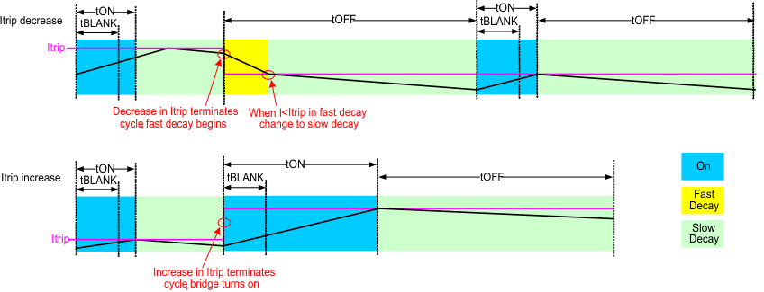 Figure 11. Itrip Level Changing During a PWM Cycle
To accurately detect zero current, an internal offset has been intentionally placed in the zero current detection circuit. If an external filter is placed on the current sense resistor to the xISENN and xISENP pins, symmetry must be maintained. This means that any resistance between the bottom of the RISENSE resistor and xISENN must be matched by the same resistor value (1% tolerance) between the top of the RISENSE resistor and xISENP. Ensure a maximum resistance of 500 Ω. The capacitor value should be chosen such that the RC time constant is between 50 ns and 60 ns. Any external filtering on these pins is optional and not required for operation.
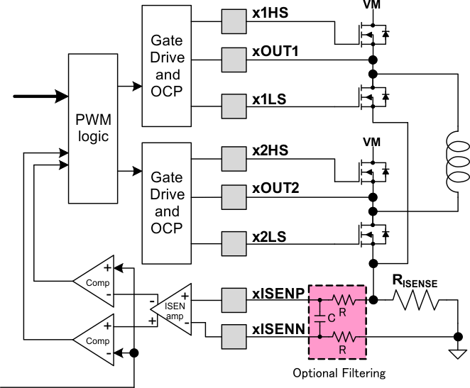 Figure 12. Optional Filtering Between RISENSE and xINSENx
7.3.6 Blanking Time
After the current is enabled in an H-bridge, the voltage on the ISEN pin is ignored for a period of time before enabling the current sense circuitry. This blanking time is adjustable from 1 µS to 5.12 µs, in 20 ns increments, by setting the TBLANK bits in the BLANK register. Note that the blanking time also sets the minimum on time of the PWM.
The same blanking time is applied to the fast decay period in auto decay mode. The PWM will ignore any transitions on Itrip after entering fast decay mode, until the blanking time has expired.
To provide better current control at very low current steps, an adaptive blanking time mode can be enabled by setting the ABT bit in the BLANK register. If ABT is set, at current levels below 30% of full scale current (as determined by the step table), the blanking time (so also the minimum on time) is cut in half, to 50% of the value programmed by the TBLANK bits.
For higher degrees of micro-stepping, TI recommends enabling ABT bit for better current regulation.
7.3.7 Predrivers
An internal charge pump circuit and predrivers inside the DRV8711 directly drive N-channel MOSFETs, which drive the motor current.
The peak drive current of the predrivers is adjustable by setting the bits in the DRIVE register. Peak source currents may be set to 50 mA, 100 mA, 150 mA, or 200 mA. The peak sink current is approximately 2x the peak source current. Adjusting the peak current will change the output slew rate, which also depends on the FET input capacitance and gate charge.
When changing the state of the output, the peak current is applied for a short period of time (tDRIVE), to charge the gate capacitance. After this time, a weak current source is used to keep the gate at the desired state. When selecting the gate drive strength for a given external FET, the selected current must be high enough to fully charge and discharge the gate during the time when driven at full current, or excessive power will be dissipated in the FET.
During high-side turnon, the low-side gate is pulled low. This prevents the gate-source capacitance of the low-side FET from inducing turnon.
The predriver circuits include enforcement of a dead time in analog circuitry, which prevents the high-side and low-side FETs from conducting at the same time. Additional dead time is added with digital delays. This delay can be selected by setting the DTIME bits in the CTRL register.
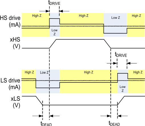 Figure 13. Predrivers
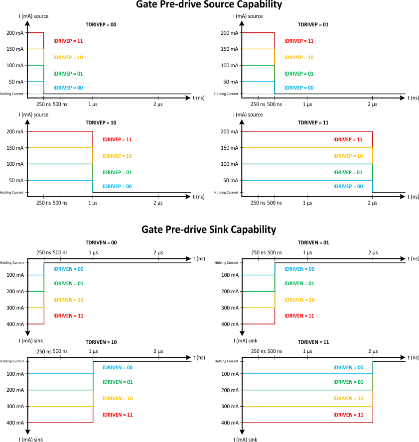 Figure 14. Gate Pre-Drive Source/Sink Capability
7.3.8 Configuring Predrivers
IDRIVE and TDRIVE are selected based on the size of external FETs used. These registers need to be configured so that the FET gates are charged completely during TDRIVE. If IDRIVE and TDRIVE are chosen to be too low for a given FET, then the FET may not turn on completely. TI suggests adjusting these values in-system with the required external FETs and stepper motor to determine the best possible setting for any application.
TDRIVE will not increase the PWM time or change the PWM chopping frequency.
In a system with capacitor charge Q and desired rise time RT, IDRIVE and TDRIVE can be initially selected based on:
IDRIVE > Q / RT
TDRIVE > 2 × RT
For best results, select the smallest IDRIVE and TDRIVE that meet the above conditions.
Example:
If the gate charge is 15 nC and the desired rise time is 400 ns, then select:
IDRIVEP = 50 mA, IDRIVEN = 100 mA
TDRIVEP = TDRIVEN = 1 µs
7.3.9 External FET Selection
In a typical setup, the DRV8711 can support external FETs over 50 nC each. However, this capacity can be lower or higher based on the device operation. For an accurate calculation of FET driving capacity, use the following equation.

Example:
If a DTIME is set to 0 (400 ns), TBLANK is set to 0 (1 µs), and TOFF is set to 0 (500 ns), then the DRV8711 will support Q < 11.5 nC FETs (this is an absolute worst-case scenario with a PWM frequency
approximately 430 kHz).
If a DTIME is set to 0 (400 ns), TBLANK is set to 0 (1 µs), and TOFF is set to 0x14 (10 µs), then the DRV8711 will support Q < 59 nC FETs (PWM frequency approximately 85 kHz).
If a DTIME is set to 0 (400 ns), TBLANK is set to 0 (1 µs), and TOFF is set to 0x60 (48 µs), then the DRV8711 will support Q < 249 nC FETs (PWM frequency approximately 20 kHz).
7.3.10 Stall Detection
The DRV8711 implements a back EMF monitoring scheme that is capable of detecting a stall during stepper motor motion. This stall detection is intended to be used to get an indication when a motor is run into a mechanical stop, or when an increased torque load on the motor causes it to stall.
To determine that a stall has occurred, a drop in motor back EMF is detected. The DRV8711 supports two methods of this detection: an automatic internal stall detection circuit, or the ability to use an external microcontroller to monitor back EMF.
During a zero-current step, one side of the H-bridge is placed in a high impedance state, and the opposite low-side FET is turned on for a brief duration defined by TORQUE register SMPLTH bit [10:8]. This allows the current to decay quickly through the low-side FET and the opposite body diode. Which side of the bridge is tri-state and which one is driven low depends on the current direction on the previous step. The bridge with the high side that has been actively PWMed (at the beginning of the PWM cycle during blank time) before entering the zero-current step will be held low and the opposite side will be tri-stated.
Back EMF is sampled on the tri-stated output pin at the end of SMPLTH time (TORQUE register bit [10:8]). The back EMF from the selected pin is divided by 4, 8, 16, or 32, depending on the setting of the VDIV bits in the STALL register. The voltage is buffered and held on an external capacitor placed on the BEMF pin. The signal on the BEMF output pin can be further processed by a microcontroller to implement more advanced control and stall detection algorithms.
The SMPLTH bit [10] is a write-only bit. When read, the bit always reads 0. TI recommends to maintain the value of the bit locally. When a change in the TORQUE register is desired, the bit can be read locally and added to the other bits to complete the value.
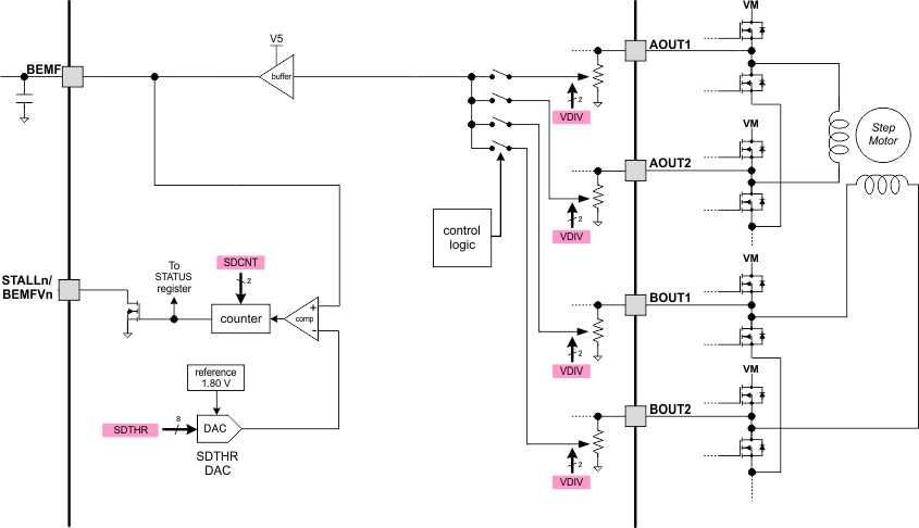 Figure 15. Stall Detection
7.3.10.1 Internal Stall Detection
To use internal stall detection, the EXSTALL bit in the CTRL register is set to 0. In this mode, the STALLn/BEMFVn output pin is used to signal a valid stall condition.
The time between step inputs must be greater than SMPLTH time for back EMF sampling.
Using internal stall detection, a stall is detected when the sampled back EMF drops below the value set by the SDTHR bits in the STALL register. A programmable counter circuit allows the assertion of the STALLn output to be delayed until the back EMF has been sampled below the SDTHR value for more than one zero-current step. The counter is programmed by the SDCNT bits in the STALL register, and provides selections of 1, 2, 4, or 8 steps.
When the stall is detected (at the end of a SMPLTH interval), the STALLn/BEMFVn pin is driven active low, and the STD bit and the STDLAT bit in the STATUS register are set. The STALLn/BEMFVn pin will deassert and the STD bit will automatically clear at the next zero-current step if a stall condition is not detected, while the STDLAT bit will remain set until a 0 is written to it. The STDLAT is reset when the STD bit clears after the first zero-cross step that does not detect a stall condition.
This stall detection scheme is only effective when the motor is stalled while running at or above some minimum speed. Because it relies on detecting a drop in motor back EMF, the motor must be rotating with sufficient speed to generate a detectable back EMF. During motor start-up, and at very slow step rates, the stall detection is not reliable.
Because back EMF can only be sampled during a zero-current state, stall detection is not possible in full step mode. During full-step operation, the stall detect circuit is gated off to prevent false signaling of a stall.
The correct setting of the SDTHR bits needs to be determined experimentally. It is dependent on many factors, including the electrical and mechanical characteristics of the load, the peak current setting, and the supply voltage.
7.3.10.2 External Stall Detection
To use an external microcontroller to manage stall detection, the EXSTALL bit in the CTRL register is set to 1. In this mode, the STALLn / BEMFVn output pin is used to signal a valid back EMF measurement is ready. In addition, the SDT and SDTLAT bits are also set at this time.
BEMFVn and BEMF are still valid outputs in this mode even if the step time is smaller than SMPLTH time.
When the BEMFVn pin goes active low, it is an indication that a valid back EMF voltage measurement is available. This signal could be used, for example, to trigger an interrupt on a microcontroller. The microcontroller can then sample the voltage present (using an A/D converter) on the BEMF pin.
After sampling the back EMF voltage, the microcontroller writes a 0 to the SDTLAT bit to clear the SDT bit and BEMFVn pin, in preparation for the next back EMF sample. If the SDTLAT bit is not cleared by the microcontroller, it will automatically be cleared in the next zero-current step.
For either internal or external stall detection, at very high motor speeds when the PWM duty cycle approaches 100%, the inductance of the motor and the short duration of each step may cause the time required for current recirculation to exceed the step time. In this case, back EMF will not be correctly sampled, and stall detection cannot function. This condition occurs most at high degrees of micro-stepping, because the zero current step lasts for a shorter duration. It is advisable to run the motor at lower degrees of micro-stepping at higher speeds to allow time for current recirculation if stall detection is needed in this condition.
7.3.11 Protection Circuits
The DRV8711 is fully protected against undervoltage, overcurrent and overtemperature events.
7.3.11.1 Overcurrent Protection (OCP)
Overcurrent is sensed by monitoring the voltage drop across the external FETs. If the voltage across a driven FET exceeds the value programmed by the OCPTH bits in the DRIVE register for more than the time period specified by the OCPDEG bits in the DRIVE register, an OCP event is recognized. When operating in direct PWM mode, during an OCP event, the H-bridge experiencing the OCP event is disabled; if operating in indexer mode, both H-bridges will be disabled. In addition, the corresponding xOCP bit in the STATUS register is set, and the FAULTn pin is driven low. The H-bridge(s) will remain off, and the xOCP bit will remain set, until it is written to 0, or the device is reset.
7.3.11.2 Predriver Fault
In PWM mode, if excessive current is detected on the gate drive outputs (which would be indicative of a failed/shorted output FET or PCB fault), the H-bridge experiencing the fault is disabled, the xPDF bit in the STATUS register is set, and the FAULTn pin is driven low. The H-bridge will remain off, and the xPDF bit will remain set until it is written to 0 or the device is reset.
When in indexer mode, both H-bridges are disabled, the xPDF bit in the STATUS register is set, and the FAULTn pin is driven low. The H-bridges will remain off, and the xPDF bit will remain set until it is written to 0 or the device is reset.
7.3.11.3 Thermal Shutdown (TSD)
If the die temperature exceeds safe limits, all FETs in the H-bridge will be disabled, the OTS bit in the STATUS register will be set, and the FAULTn pin will be driven low. Once the die temperature has fallen to a safe level operation will automatically resume and the OTS bit will reset. The FAULTn pin will be released after operation has resumed.
7.3.11.4 Undervoltage Lockout (UVLO)
If at any time the voltage on the VM pin falls below the undervoltage lockout threshold voltage, all FETs in the H-bridge will be disabled, the UVLO bit in the STATUS register will be set, and the FAULTn pin will be driven low. Operation will resume when VM rises above the UVLO threshold. The UVLO bit will remain set until it is written to 0. The FAULTn pin will be released after operation has resumed.
During any of these fault conditions, the STEP input pin will be ignored.
7.4 Device Functional Modes
7.4.1 RESET and SLEEPn Operation
An internal power-up reset circuit monitors the voltage applied to the VM pin. If VM falls below the VM undervoltage lockout voltage, the part is reset, as described below for the case of asserting the RESET pin.
If the RESET pin is asserted, all internal logic including the indexer is reset. All registers are returned to their initial default conditions. The power stage will be disabled, and all inputs, including STEP and the serial interface, are ignored when RESET is active.
On exiting reset state, some time (approximately 1 mS) needs to pass before the part is fully functional.
Applying an active low input to the SLEEPn input pin will place the device into a low power state. In sleep mode, the motor driver circuitry is disabled, the gate drive regulator and charge pump are disabled, and all analog circuitry is placed into a low power state. The digital circuitry in the device still operates, so the device registers can still be accessed via the serial interface.
When SLEEPn is active, the RESET pin does not function. SLEEPn must be exited before RESET will take effect. SLEEPn must also be exited to clear the UVLO bit in the status register.
When exiting from sleep mode, some time (approximately 1 mS) needs to pass before applying a STEP input, to allow the internal circuitry to stabilize.
7.4.2 Microstepping Drive Current
Figure 16 shows examples of stepper motor current in one of the windings. Because these waveforms are dependent on DRV8711 register settings as well as the external FETs, sense resistor, and stepper motor, they should only be used as a reference.
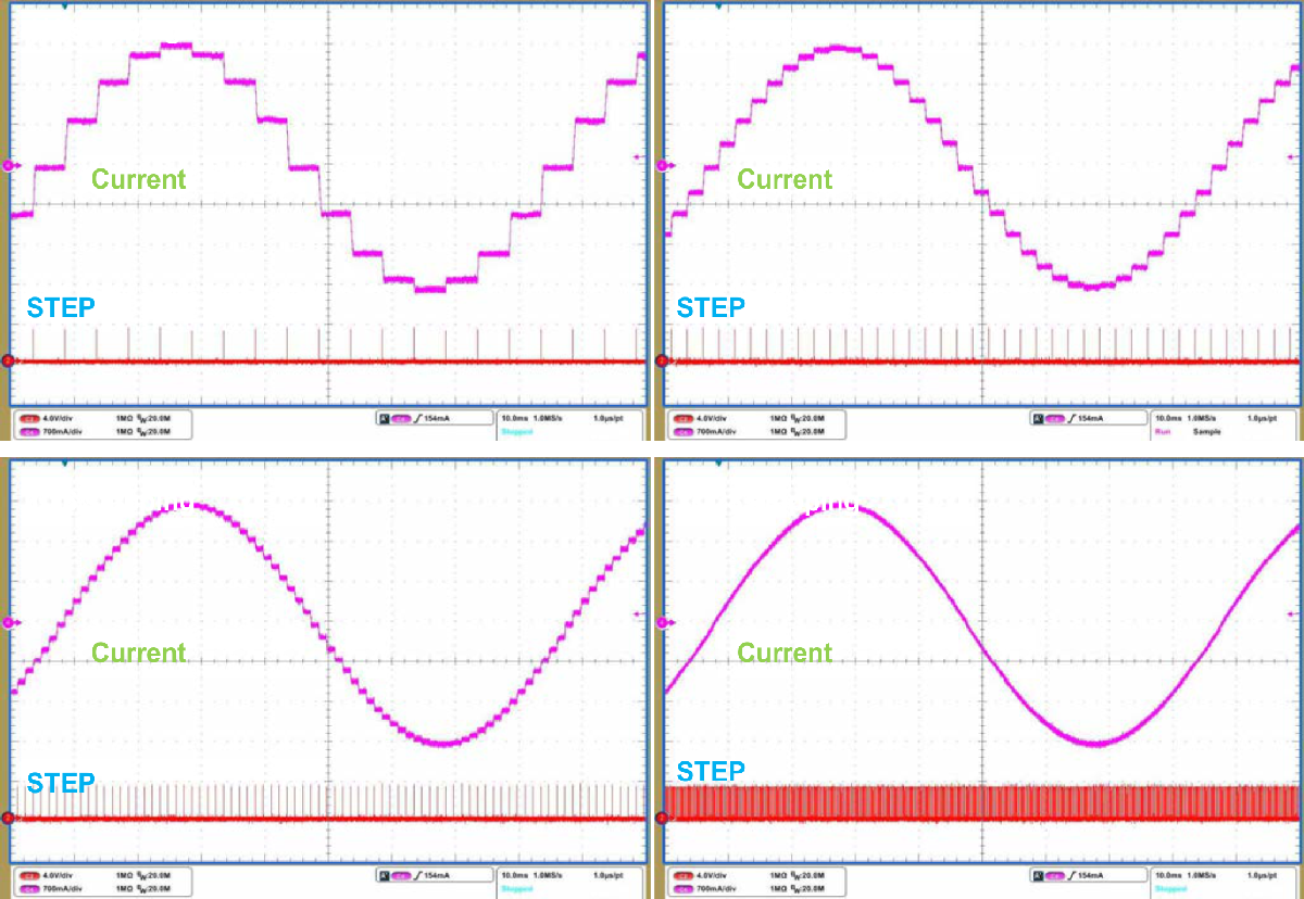 Figure 16. Microstepping Drive Current
7.5 Programming
7.5.1 Serial Data Format
The serial data consists of a 16-bit serial write, with a read/write bit, 3 address bits and 12 data bits. The 3 address bits identify one of the registers defined in the register section above. To complete the read or write transaction, SCS must be set to a logic 0.
To write to a register, data is shifted in after the address as shown in the timing diagram below. The first bit at the beginning of the access must be logic low for a write operation.

Data may be read from the registers through the SDATO pin. During a read operation, only the address is used form the SDATI pin; the data bits following are ignored. The first bit at the beginning of the access must be logic high for a read operation.

7.6 Register Maps
7.6.1 Control Registers
The DRV8711 uses internal registers to control the operation of the motor. The registers are programmed through a serial SPI communications interface. At power up or reset, the registers will be preloaded with default values as shown in CTRL Register (Address = 0x00) to STATUS Register (Address = 0x07).
Figure 19 is a map of the DRV8711 registers.
Individual register contents are defined in CTRL Register (Address = 0x00) to STATUS Register (Address = 0x07).
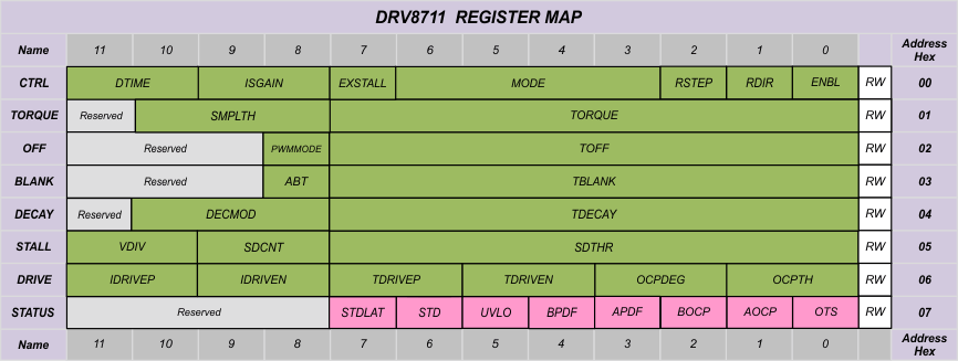 Figure 19. DRV8711 Register Map
7.6.2 CTRL Register (Address = 0x00)
| BIT | NAME | SIZE | R/W | DEFAULT | DESCRIPTION |
|---|---|---|---|---|---|
| 0 | ENBL | 1 | R/W | 0 | 0: Disable motor
1: Enable motor |
| 1 | RDIR | 1 | R/W | 0 | 0: Direction set by DIR pin
1: Direction set by inverse of DIR pin |
| 2 | RSTEP | 1 | W | 0 | 0: No action 1: Indexer will advance one step; automatically cleared after write |
| 6-3 | MODE | 4 | R/W | 0010 | 0000: Full-step, 71% current 0001: Half step 0010: 1/4 step 0011: 1/8 step 0100: 1/16 step 0101: 1/32 step 0110: 1/64 step 0111: 1/128 step 1000: 1/256 step 1001 – 1111: Reserved |
| 7 | EXSTALL | 1 | R/W | 0 | 0: Internal stall detect
1: External stall detect |
| 9-8 | ISGAIN | 2 | R/W | 00 | ISENSE amplifier gain set 00: Gain of 5 01: Gain of 10 10: Gain of 20 11: Gain of 40 |
| 11-10 | DTIME | 2 | R/W | 11 | Dead time set 00: 400 ns dead time 01: 450 ns dead time 10: 650 ns dead time 11: 850 ns dead time |
7.6.3 TORQUE Register (Address = 0x01)
| BIT | NAME | SIZE | R/W | DEFAULT | DESCRIPTION |
|---|---|---|---|---|---|
| 7-0 | TORQUE | 8 | R/W | 0xFF | Sets full-scale output current for both H-bridges |
| 10-8 | SMPLTH(1) | 3 | R/W | 001 | Back EMF sample threshold 000: 50 µs 001: 100 µs 010: 200 µs 011: 300 µs 100: 400 µs 101: 600 µs 110: 800 µs 111: 1000 µs |
| 11 | Reserved | 1 | - | - | Reserved |
7.6.4 OFF Register (Address = 0x02)
| BIT | NAME | SIZE | R/W | DEFAULT | DESCRIPTION |
|---|---|---|---|---|---|
| 7-0 | TOFF | 8 | R/W | 0x30 | Sets fixed off time, in increments of 500 ns 0x00: 500 ns 0xFF: 128 µs |
| 8 | PWMMODE | 1 | R/W | 0 | 0: Use internal indexer
1: Bypass indexer, use xINx inputs to control outputs |
| 11-9 | Reserved | 3 | - | - | Reserved |
7.6.5 BLANK Register (Address = 0x03)
| BIT | NAME | SIZE | R/W | DEFAULT | DESCRIPTION |
|---|---|---|---|---|---|
| 7-0 | TBLANK | 8 | R/W | 0x80 | Sets current trip blanking time, in increments of 20 ns 0x00: 1 µs … 0x32: 1 µs 0x33: 1.02 µs … 0xFE: 5.10 µs 0xFF: 5.12 µs Also sets minimum on-time of PWM |
| 8 | ABT | 1 | R/W | 0 | 0: Disable adaptive blanking time
1: Enable adaptive blanking time |
| 11-9 | Reserved | 3 | - | - | Reserved |
7.6.6 DECAY Register (Address = 0x04)
| BIT | NAME | SIZE | R/W | DEFAULT | DESCRIPTION |
|---|---|---|---|---|---|
| 7-0 | TDECAY | 8 | R/W | 0x10 | Sets mixed decay transition time, in increments of 500 ns |
| 10-8 | DECMOD | 3 | R/W | 001 | 000: Force slow decay at all times 001: Slow decay for increasing current, mixed decay for decreasing current (indexer mode only) 010: Force fast decay at all times 011: Use mixed decay at all times 100: Slow decay for increasing current, auto mixed decay for decreasing current (indexer mode only) 101: Use auto mixed decay at all times 110 – 111: Reserved |
| 11 | Reserved | 1 | - | - | Reserved |