ZHCSB92G June 2013 – May 2017 DRV8711
PRODUCTION DATA.
- 1 特性
- 2 应用
- 3 说明
- 4 修订历史记录
- 5 Pin Configuration and Functions
- 6 Specifications
-
7 Detailed Description
- 7.1 Overview
- 7.2 Functional Block Diagram
- 7.3 Feature Description
- 7.4 Device Functional Modes
- 7.5 Programming
- 7.6
Register Maps
- 7.6.1 Control Registers
- 7.6.2 CTRL Register (Address = 0x00)
- 7.6.3 TORQUE Register (Address = 0x01)
- 7.6.4 OFF Register (Address = 0x02)
- 7.6.5 BLANK Register (Address = 0x03)
- 7.6.6 DECAY Register (Address = 0x04)
- 7.6.7 STALL Register (Address = 0x05)
- 7.6.8 DRIVE Register (Address = 0x06)
- 7.6.9 STATUS Register (Address = 0x07)
- 8 Application and Implementation
- 9 Power Supply Recommendations
- 10Layout
- 11器件和文档支持
- 12机械、封装和可订购信息
10 Layout
10.1 Layout Guidelines
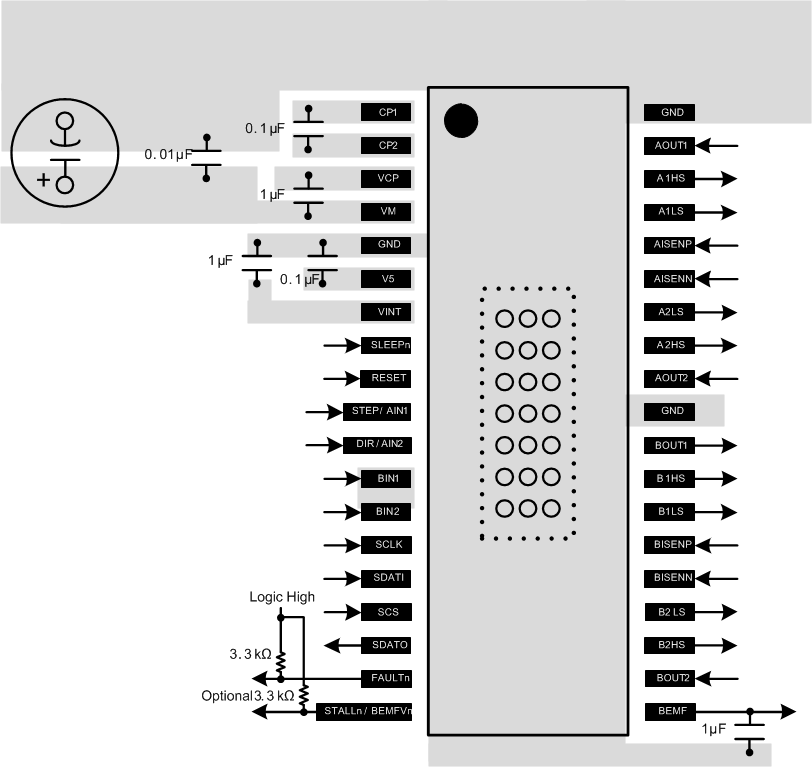
The VM pin should be bypassed to GND using low-ESR ceramic bypass capacitors with a recommended value of 0.01-μF rated for VM. This capacitor should be placed as close to the VM pin as possible with a thick trace or ground plane connection to the device GND pin. The VM pin must be bypassed to ground using an appropriate bulk capacitor. This component may be an electrolytic and should be located close to the DRV8711.
A low-ESR ceramic capacitor must be placed in between the VM and VCP pins. TI recommends a value of 1 μF rated for 16 V. Place this component as close to the pins as possible.
A low-ESR ceramic capacitor must be placed in between the CP1 and CP2 pins. TI recommends a value of 0.1 μF rated for VM. Place this component as close to the pins as possible.
Bypass VINT to ground with a 1-μF ceramic capacitor rated 6.3 V. Place this bypass capacitor as close to the pin as possible.
Bypass V5 to ground with a 1-μF ceramic capacitor rated 10 V. Place this bypass capacitor as close to the pin as possible.
10.2 Layout Example
 Figure 24. Recommended Layout Example