ZHCSDO0A March 2015 – May 2015 DRV8701
PRODUCTION DATA.
- 1 特性
- 2 应用
- 3 说明
- 4 修订历史记录
- 5 Pin Configuration and Functions
- 6 Specifications
-
7 Detailed Description
- 7.1 Overview
- 7.2 Functional Block Diagram
- 7.3
Feature Description
- 7.3.1 Bridge Control
- 7.3.2 Half-Bridge Operation
- 7.3.3 Current Regulation
- 7.3.4 Amplifier Output SO
- 7.3.5 PWM Motor Gate Drivers
- 7.3.6 IDRIVE Pin
- 7.3.7 Dead Time
- 7.3.8 Propagation Delay
- 7.3.9 Overcurrent VDS Monitor
- 7.3.10 Charge Pump
- 7.3.11 LDO Voltage Regulators
- 7.3.12 Gate Drive Clamp
- 7.3.13 Protection Circuits
- 7.3.14 Reverse Supply Protection
- 7.4 Device Functional Modes
- 8 Application and Implementation
- 9 Power Supply Recommendations
- 10Layout
- 11器件和文档支持
- 12机械、封装和可订购信息
8 Application and Implementation
NOTE
Information in the following applications sections is not part of the TI component specification, and TI does not warrant its accuracy or completeness. TI’s customers are responsible for determining suitability of components for their purposes. Customers should validate and test their design implementation to confirm system functionality.
8.1 Application Information
The DRV8701 is used in brushed-DC, solenoid, or relay control.
8.2 Typical Applications
8.2.1 Brushed-DC Motor Control
The following design procedure can be used to configure the DRV8701.
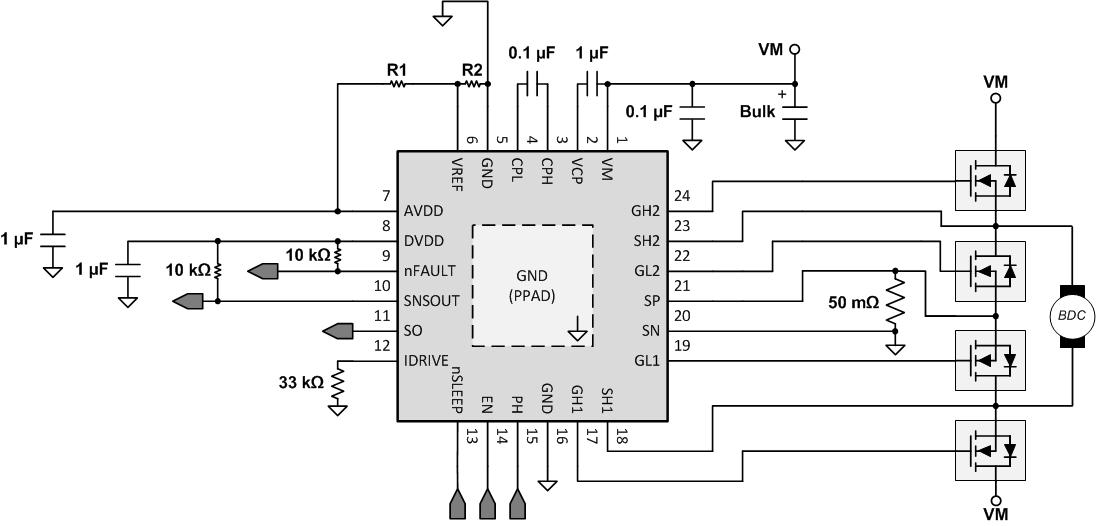 Figure 34. Typical Application Schematic
8.2.1.1 Design Requirements
Table 10 gives design input parameters for system design.
Table 10. Design Parameters
| Design Parameter | Reference | Example Value |
|---|---|---|
| Nominal supply voltage | VM | 18 V |
| Supply voltage range | VMMIN, VMMAX | 12 to 24 V |
| FET total gate charge(1) | QG | 14 nC (typically) |
| FET gate-to-drain charge(1) | QGD | 2.3 nC (typically) |
| Target FET gate rise time | RT | 100 to 300 ns |
| Motor current chopping level | ICHOP | 3 A |
8.2.1.2 Detailed Design Procedure
8.2.1.2.1 External FET Selection
The DRV8701 FET support is based on the charge pump capacity and output PWM frequency. For a quick calculation of FET driving capacity, use the following equations when drive and brake (slow decay) are the primary modes of operation:

where
- fPWM is the maximum desired PWM frequency to be applied to the DRV8701 inputs or the current chopping frequency, whichever is larger.
- IVCP is the charge pump capacity, which depends on VM.
The internal current chopping frequency is at most:

Example: If a system at VM = 7 V (IVCP = 8 mA) uses a maximum PWM frequency of 40 kHz, then the DRV8701 will support QG < 200 nC FETs.
If the application will require a forced fast decay (or alternating between drive and reverse drive), the maximum FET driving capacity is given by:

8.2.1.2.2 IDRIVE Configuration
Select IDRIVE based on the gate charge of the FETs. Configure this pin so that the FET gates are charged completely during tDRIVE. If the designer chooses an IDRIVE that is too low for a given FET, then the FET may not turn on completely. TI suggests to adjust these values in-system with the required external FETs and motor to determine the best possible setting for any application.
For FETs with a known gate-to-drain charge (QGD) and desired rise time (RT), select IDRIVE based on:

Example: If the gate-to-drain charge is 2.3 nC, and the desired rise time is around 100 to 300 ns,
IDRIVE1 = 2.3 nC / 100 ns = 23 mA
IDRIVE2 = 2.3 nC / 300 ns = 7.7 mA
Select IDRIVE between 7.7 and 23 mA
Select IDRIVE as 12.5-mA source (25-mA sink)
Requires a 33-kΩ resistor from the IDRIVE pin to GND
8.2.1.2.3 Current Chopping Configuration
The chopping current is set based on the sense resistor value and the analog voltage at VREF. Calculate the current using Equation 9. The amplifier gain AV is 20 V/V and VOFF is typically 50 mV.
Example: If the desired chopping current is 3 A,
Set RSENSE = 50 mΩ

VREF would have to be 3.05 V.
Create a resistor divider from AVDD (4.8 V) to set VREF ≈ 3 V
Set R2 = 3.3 kΩ; set R1 = 2 kΩ.
8.2.1.3 Application Curves
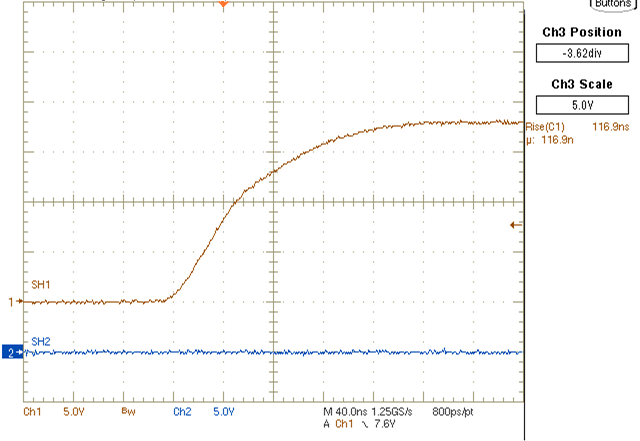 Figure 35. SH1 Rise Time (12.5-mA Source, 25-mA Sink)
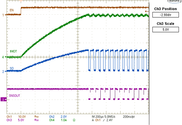 Figure 37. Current Regulating at 3 A on Motor Startup
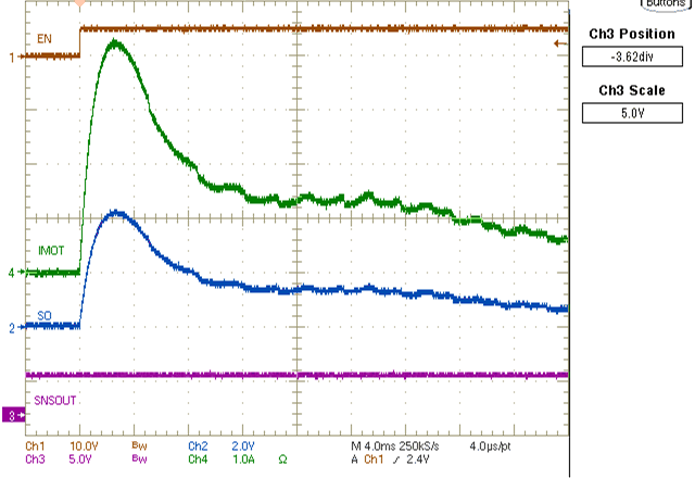 Figure 39. Current Profile on Motor Startup Without Regulation
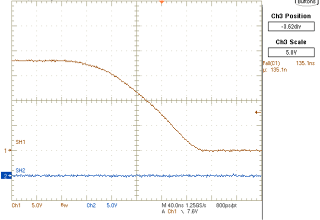 Figure 36. SH1 Fall Time (12.5-mA Source, 25-mA Sink)
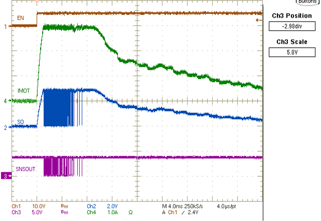 Figure 38. Current Profile on Motor Startup With Regulation
8.2.2 Alternate Application
In this example, the DRV8701 is powered from a supply that is boosted above VBAT. This allows the system to work at lower VBAT voltages, but requires the user to disable OCP monitoring.
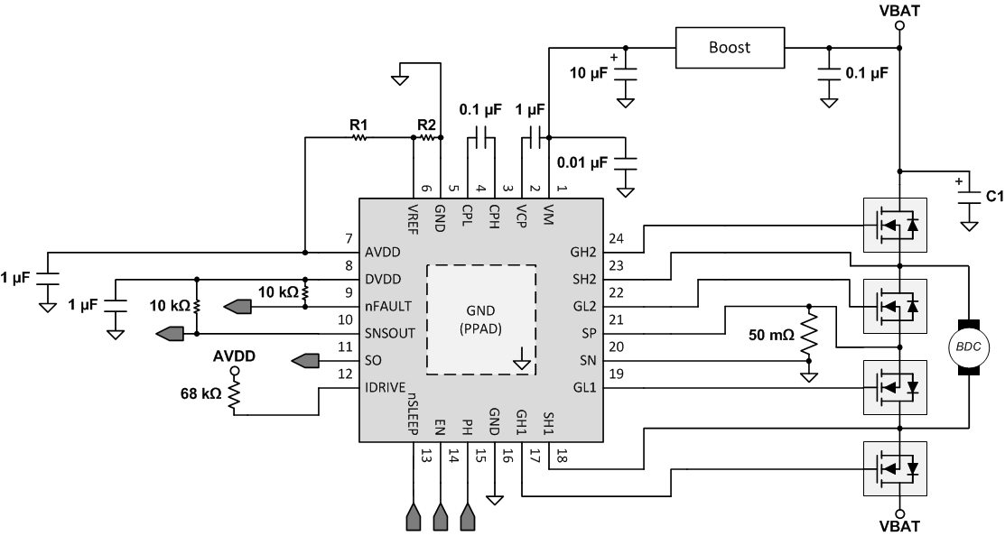 Figure 40. DRV8701 on Boosted Supply
8.2.2.1 Design Requirements
Table 11 gives design input parameters for system design.
Table 11. Design Parameters
| Design Parameter | Reference | Example Value |
|---|---|---|
| Battery voltage | VBAT | 12 V nominal Minimum operation: 4.0 V |
| DRV8701 supply voltage | VM | VM = 7 V when VBAT < 7 V VM = VBAT when VBAT ≥ 7 V |
| FET total gate charge | QG | 42 nC |
| FET gate-to-drain charge | QGD | 11 nC |
| Motor current chopping level | ICHOP | 3 A |
8.2.3 Detailed Design Procedure
8.2.3.1 IDRIVE Configuration
Because the VM supply to the DRV8701 is different from the external H-bridge supply VBAT, the designer must disable the overcurrent monitor to prevent false overcurrent detection. The designer must place a 68-kΩ resistor between the IDRIVE pin and AVDD.
IDRIVE is fixed at 25-mA source and 50-mA sink in this mode.
So, the rise time is 11 nC / 25 mA = 440 ns.
8.2.3.2 VM Boost Voltage
To determine an effective voltage to boost VM, first determine the minimum VBAT at which the system must operate. Select VM such that the gate driver clamps do not turn on during normal operation.

Example: If VBAT minimum is 4.0 V,
VM < 7.75 V
So VM = 7 V is selected to allow for adequate margin.