ZHCSG81 April 2017 DCPA10505 , DCPA10505D , DCPA10512 , DCPA10512D , DCPA10515 , DCPA10515D
PRODUCTION DATA.
- 1 特性
- 2 应用
- 3 说明
- 4 修订历史记录
- 5 Pin Configuration and Functions
-
6 Specifications
- 6.1 Absolute Maximum Ratings
- 6.2 ESD Ratings
- 6.3 Recommended Operating Conditions
- 6.4 Electrical Characteristics
- 6.5 Switching Characteristics
- 6.6 Typical Characteristics (DCPA10505)
- 6.7 Typical Characteristics (DCPA10512)
- 6.8 Typical Characteristics (DCPA10515)
- 6.9 Typical Characteristics (DCPA10505D)
- 6.10 Typical Characteristics (DCPA10512D)
- 6.11 Typical Characteristics (DCPA10515D)
-
7 Detailed Description
- 7.1 Overview
- 7.2 Functional Block Diagrams
- 7.3 Feature Description
- 8 Application and Implementation
- 9 Power Supply Recommendations
- 10Layout
- 11器件和文档支持
- 12机械、封装和可订购信息
10 Layout
10.1 Layout Guidelines
Due to the high power density of these devices, provide ground planes on the input and output rails.
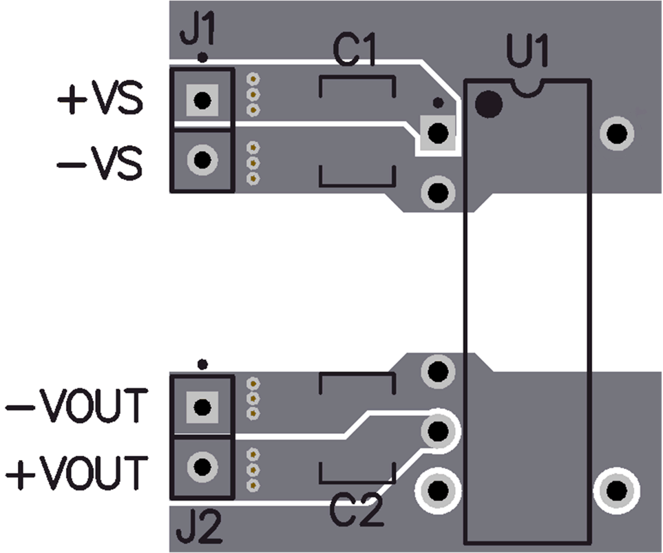
Figure 40 shows the schematic for a single output DCPA1 device. Figure 40 illustrates a printed circuit board (PCB) layout for the schematics.
Including input power and ground planes provides a low-impedance path for the input power. For the output, the COM signal connects via a ground plane, while the connections for the positive and negative voltage outputs conduct via wide traces in order to minimize losses.
The output should be taken from the device using ground and power planes, thereby ensuring minimum losses.
The location of the decoupling capacitors in close proximity to their respective pins ensures low losses due to the effects of stray inductance, thus improving the ripple performance. This location is of particular importance to the input decoupling capacitor, because this capacitor supplies the transient current associated with the fast switching waveforms of the power drive circuits.
If the SYNCIN pin is unused, it is recommended to connect this pin to the input side common, –VS. Allow the SWOUT pin, to remain configured as a floating pad.
10.2 Layout Example
 Figure 40. Typical Layout