ZHCSG99 April 2017 CDCS504-Q1
PRODUCTION DATA.
6 Specifications
6.1 Absolute Maximum Ratings
over operating free-air temperature range (unless otherwise noted)(1)| MIN | MAX | UNIT | ||
|---|---|---|---|---|
| VDD | Supply voltage | –0.5 | 4.6 | V |
| VIN | Input voltage | –0.5 | 4.6 | V |
| Vout | Output voltage | –0.5 | 4.6 | V |
| IIN | Input current (VI < 0, VI > VDD) | 20 | mA | |
| Iout | Continuous output current | 50 | mA | |
| TJ | Maximum junction temperature | 125 | °C | |
| Tstg | Storage temperature | –65 | 150 | °C |
(1) Stresses beyond those listed under Absolute Maximum Ratings may cause permanent damage to the device. These are stress ratings only and functional operation of the device at these or any other conditions beyond those indicated under Recommended Operating Conditions is not implied. Exposure to absolute-maximum-rated conditions for extended periods may affect device reliability.
6.2 ESD Ratings
| VALUE | UNIT | |||
|---|---|---|---|---|
| V(ESD) | Electrostatic discharge | Human-body model (HBM), per AEC Q100-002(1) | ±1500 | V |
| Charged-device model (CDM), per AEC Q100-011 | ±750 | |||
(1) AEC Q100-002 indicates that HBM stressing shall be in accordance with the ANSI/ESDA/JEDEC JS-001 specification.
6.3 Recommended Operating Conditions
| MIN | NOM | MAX | UNIT | |||
|---|---|---|---|---|---|---|
| VDD | Supply voltage | 3 | 3.6 | V | ||
| fIN | Input frequency | FS = 0 | 2 | 27 | MHz | |
| FS = 1 | 2 | 27 | ||||
| VIL | Low-level input voltage LVCMOS | 0.3 × VDD | V | |||
| VIH | High-level input voltage LVCMOS | 0.7 × VDD | V | |||
| VI | Input voltage threshold LVCMOS | 0.5 × VDD | V | |||
| CL | Output load test LVCMOS | 15 | pF | |||
| IOH/IOL | Output current | ±12 | mA | |||
| TA | Operating free-air temperature | –40 | 105 | °C | ||
6.4 Thermal Information
over operating free-air temperature range (unless otherwise noted)(2)| THERMAL METRIC(1) | CDCS504-Q1 | UNIT | |||
|---|---|---|---|---|---|
| PW (TSSOP) | |||||
| 8 PINS | |||||
| RθJA | Junction-to-ambient thermal resistance | 179.9 | °C/W | ||
| High K | Thermal Airflow (CFM) 0 | 149 | |||
| Thermal Airflow (CFM) 150 | 142 | ||||
| Thermal Airflow (CFM) 250 | 138 | ||||
| Thermal Airflow (CFM) 500 | 132 | ||||
| Low K | Thermal Airflow (CFM) 0 | 230 | |||
| Thermal Airflow (CFM) 150 | 185 | ||||
| Thermal Airflow (CFM) 250 | 170 | ||||
| Thermal Airflow (CFM) 500 | 150 | ||||
| RθJC(top) | Junction-to-case (top) thermal resistance | 64.9 | °C/W | ||
| High K | 65 | ||||
| Low K | 69 | ||||
| RθJB | Junction-to-board thermal resistance | 108.7 | °C/W | ||
| ψJT | Junction-to-top characterization parameter | 9 | °C/W | ||
| ψJB | Junction-to-board characterization parameter | 107 | °C/W | ||
| RθJC(bot) | Junction-to-case (bottom) thermal resistance | n/a | °C/W | ||
(1) For more information about traditional and new thermal metrics, see the Semiconductor and IC Package Thermal Metrics application report.
(2) The package thermal impedance is calculated in accordance with JESD 51 and JEDEC2S2P (high-k board).
6.5 Electrical Characteristics – Device Characteristics
over recommended operating free-air temperature range (unless otherwise noted)| PARAMETER | TEST CONDITIONS | MIN | TYP | MAX | UNIT | |
|---|---|---|---|---|---|---|
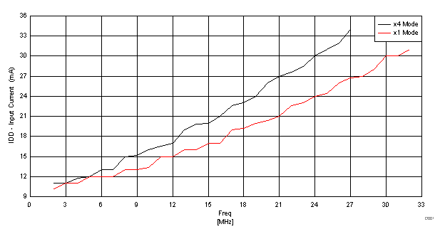
| IDD | Device supply current | fin = 3.072 MHz; FS = 1 | 24 | mA | ||
| fOUT | Output frequency | FS = 0 | 2 | 27 | MHz | |
| FS = 1 | 8 | 108 | ||||
| IIH | LVCMOS input current | VI = VDD; VDD = 3.6 V | 10 | μA | ||
| IIL | LVCMOS input current | VI = 0 V; VDD = 3.6 V | –10 | μA | ||
| VOH | LVCMOS high-level output voltage | IOH = -–0.1 mA | 2.9 | V | ||
| IOH = -–8 mA | 2.4 | |||||
| IOH = -–12 mA | 2.2 | |||||
| VOL | LVCMOS low-level output voltage | IOL = 0.1 mA | 0.1 | V | ||
| IOL = 8 mA | 0.5 | |||||
| IOL = 12 mA | 0.8 | |||||
| IOZ | High-impedance-state output current | OE = Low | –2 | 2 | μA | |
| tJIT(C-C) | Cycle to cycle jitter(1) | fout = 11.264 MHz; FS = 1, 10000 Cycles |
144 | ps | ||
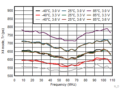
| tr | Rise time(1) | 20%–80% | 0.65 | ns | ||
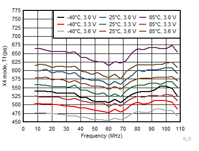
| tf | Fall time(1) | 20%–80% | 0.55 | ns | ||
| Odc | Output duty cycle(2) | 45% | 55% | |||
(1) Measured with Test Load, see Figure 4.
(2) Not production tested.
6.6 Typical Characteristics


| VCC = 3.3 V, output loaded with test load |
