ZHCSCR2 July 2014
PRODUCTION DATA.
- 1 特性
- 2 应用
- 3 说明
- 4 简化电路原理图
- 5 修订历史记录
- 6 说明(续)
- 7 Pin Configuration and Functions
-
8 Specifications
- 8.1 Absolute Maximum Ratings
- 8.2 Handling Ratings
- 8.3 Recommended Operating Conditions
- 8.4 Thermal Information
- 8.5 Electrical Characteristics: Supply Current
- 8.6 Electrical Characteristics: I/O
- 8.7 Electrical Characteristics: ADC
- 8.8 Electrical Characteristics: Power-On Reset
- 8.9 Electrical Characteristics: Oscillator
- 8.10 Electrical Characteristics: Data Flash Memory
- 8.11 Electrical Characteristics: Register Backup
- 8.12 SMBus Timing Specifications
- 8.13 Typical Characteristics
- 9 Detailed Description
- 10Application and Implementation
- 11Power Supply Recommendations
- 12Layout
- 13器件和文档支持
- 14机械封装和可订购信息
8 Specifications
8.1 Absolute Maximum Ratings
Over operating free-air temperature range (unless otherwise noted)(1)| MIN | MAX | UNIT | ||
|---|---|---|---|---|
| VCC relative to VSS | Supply voltage range | –0.3 | 2.75 | V |
| V(IOD) relative to VSS | Open-drain I/O pins | –0.3 | 6 | V |
| VI relative to VSS | Input voltage range to all other pins | –0.3 | VCC + 0.3 | V |
| TA | Operating free-air temperature range | –40 | 85 | °C |
(1) Stresses beyond those listed under absolute maximum ratings may cause permanent damage to the device. These are stress ratings only, and functional operation of the device at these or any other conditions beyond those indicated under recommended operating conditions is not implied. Exposure to absolute–maximum–rated conditions for extended periods may affect device reliability.
8.2 Handling Ratings
| MIN | MAX | UNIT | ||
|---|---|---|---|---|
| Tstg | Storage temperature range | –65 | 150 | °C |
| VESD(1) | Human Body Model (HBM) ESD stress voltage(2) | –2 | 2 | kV |
| Charged Device Model (CDM) ESD stress voltage(3) | –500 | 500 | V | |
(1) Electrostatic discharge (ESD) that measures device sensitivity and immunity to damage caused by assembly line electrostatic discharges into the device.
(2) Level listed above is the passing level per ANSI/ESDA/JEDEC JS-001. JEDEC document JEP155 states that 500-V HBM enables safe manufacturing with a standard ESD control process. Pins listed as 1000 V may actually have a higher performance.
(3) Level listed above is the passing level per EIA-JEDEC JESD22-C101. JEDEC document JEP157 states that 250-V CDM enables safe manufacturing with a standard ESD control process. Pins listed as 250 V may actually have a higher performance.
8.3 Recommended Operating Conditions
VCC = 2.4 V to 2.6 V, TA = –40°C to 85°C (unless otherwise noted)| PARAMETER | TEST CONDITIONS | MIN | TYP | MAX | UNIT | |
|---|---|---|---|---|---|---|
| VCC | Supply voltage | 2.4 | 2.5 | 2.6 | V | |
| VO | Output voltage range | SAFE | VCC | |||
| SMBC, SMBD, VEN | 5.5 | V | ||||
| ADREN, GPIO A, GPIO B, SDATA, SCLK, PWRM, LED1...5 (when used as GPO) | VCC | |||||
| VIN | Input voltage range | BAT, VAUX, SMBA | 1 | V | ||
| SMBD, SMBC, ALERT, DISP, PRES, KEYIN | 5.5 | |||||
| SDATA, GPIO A, GPIO B, LED1...5 (when used as GPI) | VCC | |||||
| TOPR | Operating Temperature | –40 | 85 | °C | ||
8.4 Thermal Information
| THERMAL METRIC(1) | bq78350 | UNIT | ||
|---|---|---|---|---|
| TSSOP (DBT) | QFN (RSM) | |||
| 30 PINS | 32 PINS | |||
| RJA, High K | Junction-to-ambient thermal resistance(2) | 81.4 | 37.4 | °C/W |
| RJC(top) | Junction-to-case(top) thermal resistance(3) | 16.2 | 30.6 | |
| RJB | Junction-to-board thermal resistance(4) | 34.1 | 7.7 | |
| ψJT | Junction-to-top characterization parameter(5) | 0.4 | 0.4 | |
| ψJB | Junction-to-board characterization parameter(6) | 33.6 | 7.5 | |
| RθJC(bottom) | Junction-to-case(bottom) thermal resistance(7) | n/a | 2.6 | |
(1) For more information about traditional and new thermal metrics, see the IC Package Thermal Metrics application report, SPRA953.
(2) The junction-to-ambient thermal resistance under natural convection is obtained in a simulation on a JEDEC-standard, high-K board, as specified in JESD51-7, in an environment described in JESD51-2a.
(3) The junction-to-case (top) thermal resistance is obtained by simulating a cold plate test on the package top. No specific JEDEC-standard test exists, but a close description can be found in the ANSI SEMI standard G30-88.
(4) The junction-to-board thermal resistance is obtained by simulating in an environment with a ring cold plate fixture to control the PCB temperature, as described in JESD51-8.
(5) The junction-to-top characterization parameter, ψJT, estimates the junction temperature of a device in a real system and is extracted from the simulation data for obtaining θJA, using a procedure described in JESD51-2a (sections 6 and 7).
(6) The junction-to-board characterization parameter, ψJB, estimates the junction temperature of a device in a real system and is extracted from the simulation data for obtaining θJA , using a procedure described in JESD51-2a (sections 6 and 7).
(7) The junction-to-case (bottom) thermal resistance is obtained by simulating a cold plate test on the exposed (power) pad. No specific JEDEC standard test exists, but a close description can be found in the ANSI SEMI standard G30-88.
8.5 Electrical Characteristics: Supply Current
VCC = 2.4 V to 2.6 V, TA = –40°C to 85°C (unless otherwise noted)| PARAMETER | TEST CONDITIONS | MIN | TYP | MAX | UNIT | |
|---|---|---|---|---|---|---|
| ICC | Operating mode current | No flash programming | 650(1) | μA | ||
| I(SLEEP) | Low-power storage mode current | SLEEP mode | 300(2) | μA | ||
| I(SHUTDOWN) | Low-power SHUTDOWN mode current | SHUTDOWN mode | 0.1 | 1 | μA | |
(1) The actual current consumption of this mode fluctuates during operation over a 1-s period. The value shown is an average using the default data flash configuration.
(2) The actual current consumption of this mode fluctuates during operation over a user-configurable period. The value shown is an average using the default data flash configuration.
8.6 Electrical Characteristics: I/O
VCC = 2.4 V to 2.6 V, TA = –40°C to 85°C (unless otherwise noted)| PARAMETER | TEST CONDITIONS | MIN | TYP | MAX | UNIT | |
|---|---|---|---|---|---|---|
| VOL | Output voltage low SMBC, SMBD, SDATA, SCLK, SAFE, ADREN, VEN, GPIO A, GPIO B, PWRM | IOL = 0.5 mA | 0.4 | V | ||
| Output voltage low LED1, LED2, LED3, LED4, LED5 | IOL = 3 mA | 0.4 | ||||
| VOH | Output voltage high SMBC, SMBD, SDATA, SCLK, SAFE, ADREN, VEN, GPIO A, GPIO B, PWRM | IOH = –1 mA | VCC – 0.5 | V | ||
| VIL | Input voltage low SMBC, SMBD, SDATA, SCLK, ALERT, DISP, SMBA, GPIO A, GPIO B, PRES, KEYIN | –0.3 | 0.8 | V | ||
| VIH | Input voltage high SMBC, SMBD, SDATA, SCLK, ALERT, SMBA, GPIO A, GPIO B | 2 | 6 | V | ||
| Input voltage high DISP, PRES, KEYIN | 2 | VCC + 0.3 | V | |||
| CIN | Input capacitance | 5 | pF | |||
| ILKG | Input leakage current | 1 | µA | |||
8.7 Electrical Characteristics: ADC
VCC = 2.4 V to 2.6 V, TA = –40°C to 85°C (unless otherwise noted)| PARAMETER | TEST CONDITIONS | MIN | TYP | MAX | UNIT |
|---|---|---|---|---|---|
| Input voltage range | BAT, VAUX | –0.2 | 1 | V | |
| Conversion time | 31.5 | ms | |||
| Resolution (no missing codes) | 16 | bits | |||
| Effective resolution | 14 | 15 | bits | ||
| Integral nonlinearity | ±0.03% | FSR(1) | |||
| Offset error(2) | 140 | 250 | µV | ||
| Offset error drift(2) | TA = 25°C to 85°C | 2.5 | 18 | V/°C | |
| Full-scale error(3) | ±0.1% | ±0.7% | |||
| Full-scale error drift | 50 | PPM/°C | |||
| Effective input resistance(4) | 8 | MΩ |
(1) Full-scale reference
(2) Post-calibration performance and no I/O changes during conversion with SRN as the ground reference
(3) Uncalibrated performance. This gain error can be eliminated with external calibration.
(4) The A/D input is a switched-capacitor input. Since the input is switched, the effective input resistance is a measure of the average resistance.
8.8 Electrical Characteristics: Power-On Reset
VCC = 2.4 V to 2.6 V, TA = –40°C to 85°C (unless otherwise noted)| PARAMETER | TEST CONDITIONS | MIN | TYP | MAX | UNIT | |
|---|---|---|---|---|---|---|
| VIT– | Negative-going voltage input | 1.7 | 1.8 | 1.9 | V | |
| VHYS | Power-on reset hysteresis | 50 | 125 | 200 | mV | |
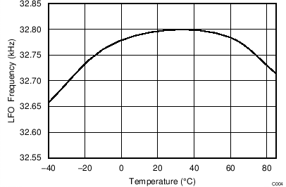
8.9 Electrical Characteristics: Oscillator
VCC = 2.4 V to 2.6 V, TA = –40°C to 85°C (unless otherwise noted)| PARAMETER | TEST CONDITIONS | MIN | TYP | MAX | UNIT | |
|---|---|---|---|---|---|---|
| f(OSC) | Operating frequency | 4.194 | MHz | |||
| f(EIO) | Frequency error(1)(2) | –3% | 0.25% | 3% | ||
| TA = 20°C to 70°C | –2 | 0.25 | 2 | |||
| t(SXO) | Start-up time(3) | 2.5 | 5 | ms | ||
| LOW FREQUENCY OSCILLATOR | ||||||
| f(LOSC) | Operating frequency | 32.768 | kHz | |||
| f(LEIO) | Frequency error(2)(4) | –2.5% | 0.25% | 2.5% | ||
| TA = 20°C to 70°C | –1.5 | 0.25 | 1.5 | |||
| t(LSXO) | Start-up time(5) | 500 | ms | |||
(1) The frequency error is measured from 4.194 MHz.
(2) The frequency drift is included and measured from the trimmed frequency at VCC = 2.5 V, TA = 25°C.
(3) The start-up time is defined as the time it takes for the oscillator output frequency to be within 1% of the specified frequency.
(4) The frequency error is measured from 32.768 kHz.
(5) The start-up time is defined as the time it takes for the oscillator output frequency to be ±3%.
8.10 Electrical Characteristics: Data Flash Memory
VCC = 2.4 V to 2.6 V, TA = –40°C to 85°C (unless otherwise noted)| PARAMETER | TEST CONDITIONS | MIN | TYP | MAX | UNIT | |
|---|---|---|---|---|---|---|
| tDR | Data retention | See note(1) | 10 | Years | ||
| Flash programming write-cycles | See note(1) | 20,000 | Cycles | |||
| t(WORDPROG) | Word programming time | See note(1) | 2 | ms | ||
| I(DDdPROG) | Flash-write supply current | See note(1) | 5 | 10 | mA | |
(1) Specified by design. Not production tested.
8.11 Electrical Characteristics: Register Backup
VCC = 2.4 V to 2.6 V, TA = –40°C to 85°C (unless otherwise noted)| PARAMETER | TEST CONDITIONS | MIN | TYP | MAX | UNIT | |
|---|---|---|---|---|---|---|
| I(RB) | RB data-retention input current | V(RB) > V(RBMIN), VCC < VIT– | 1500 | nA | ||
| V(RB) > V(RBMIN), VCC < VIT–, TA = 0°C to 50°C | 40 | 160 | ||||
| V(RB) | RB data-retention voltage (1) | 1.7 | V | |||
8.12 SMBus Timing Specifications
VCC = 2.4 V to 2.6 V, TA = –40°C to 85°C (unless otherwise noted)| PARAMETER | TEST CONDITIONS | MIN | TYP | MAX | UNIT | |
|---|---|---|---|---|---|---|
| fSMB | SMBus operating frequency | SLAVE mode, SMBC 50% duty cycle | 10 | 100 | kHz | |
| fMAS | SMBus master clock frequency | MASTER mode, no clock low slave extend | 51.2 | |||
| tBUF | Bus free time between start and stop | 4.7 | ms | |||
| tHD:STA | Hold time after (repeated) start | 4 | ||||
| tSU:STA | Repeated start setup time | 4.7 | ||||
| tSU:STO | Stop setup time | 4 | ||||
| tHD:DAT | Data hold time | RECEIVE mode | 0 | ns | ||
| TRANSMIT mode | 300 | |||||
| tSU:DAT | Data setup time | 250 | ||||
| tTIMEOUT | Error signal/detect | See note(1) | 25 | 35 | ms | |
| tLOW | Clock low period | 4.7 | µs | |||
| tHIGH | Clock high period | See note(2) | 4 | 50 | ||
| tLOW:SEXT | Cumulative clock low slave extend time | See note(3) | 25 | ms | ||
| tLOW:MEXT | Cumulative clock low master extend time | See note(4) | 10 | |||
| tF | Clock/data fall time | (VILMAX – 0.15 V) to (VIHMIN + 0.15 V) | 300 | ns | ||
| tR | Clock/data rise time | 0.9 VCC to (VILMAX – 0.15 V) | 1000 | |||
(1) The bq78350 times out when any clock low exceeds tTIMEOUT.
(2) tHIGH:MAX is minimum bus idle time. SMBC = 1 for t > 50 μs causes a reset of any transaction in progress involving the bq78350.
(3) tLOW:SEXT is the cumulative time a slave device is allowed to extend the clock cycles in one message from initial start to stop.
(4) tLOW:MEXT is the cumulative time a master device is allowed to extend the clock cycles in one message from initial start to stop.
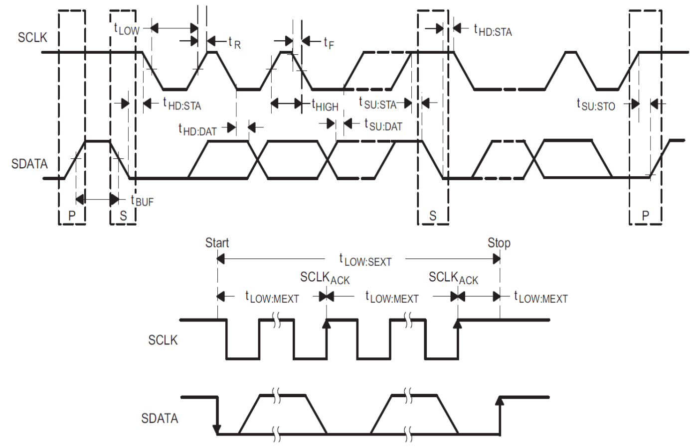 Figure 1. SMBus Timing Diagram
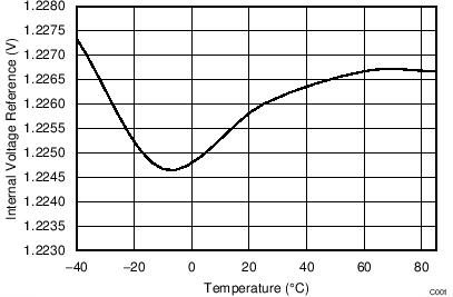
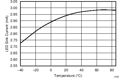
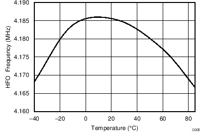
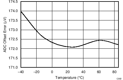
8.13 Typical Characteristics