ZHCSCR2 July 2014
PRODUCTION DATA.
- 1 特性
- 2 应用
- 3 说明
- 4 简化电路原理图
- 5 修订历史记录
- 6 说明(续)
- 7 Pin Configuration and Functions
-
8 Specifications
- 8.1 Absolute Maximum Ratings
- 8.2 Handling Ratings
- 8.3 Recommended Operating Conditions
- 8.4 Thermal Information
- 8.5 Electrical Characteristics: Supply Current
- 8.6 Electrical Characteristics: I/O
- 8.7 Electrical Characteristics: ADC
- 8.8 Electrical Characteristics: Power-On Reset
- 8.9 Electrical Characteristics: Oscillator
- 8.10 Electrical Characteristics: Data Flash Memory
- 8.11 Electrical Characteristics: Register Backup
- 8.12 SMBus Timing Specifications
- 8.13 Typical Characteristics
- 9 Detailed Description
- 10Application and Implementation
- 11Power Supply Recommendations
- 12Layout
- 13器件和文档支持
- 14机械封装和可订购信息
7 Pin Configuration and Functions
30-Pin DBT Package
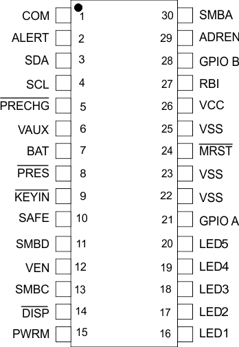
Pin Functions
| PIN | I/O(1) | DESCRIPTION | |
|---|---|---|---|
| NO. | NAME | ||
| 1 | COM | O | Open Drain Output LCD common connection |
| 2 | ALERT | I/O | Input/Output to the bq769x0 AFE |
| 3 | SDA | I/O | Data transfer to and from the bq769x0 AFE. Requires a 10-k pullup to VCC. |
| 4 | SCL | I/O | Communication clock to the bq769x0 AFE. Requires a 10-k pullup to VCC. |
| 5 | PRECHG | O | Programmable polarity (default is active low) output to enable an optional precharge FET. This pin has an internal pullup to 2.5 V when configured as active high, and is open drain when configured as active low. |
| 6 | VAUX | AI | Auxiliary voltage input |
| 7 | BAT | AI | Translated battery voltage input |
| 8 | PRES | I | Active low input to sense system insertion. This typically requires additional ESD protection. If this pin is not used, then it should be tied to VSS. |
| 9 | KEYIN | I | A low level indicates application key-switch is inactive on position. A high level causes the DSG protection FET to open. |
| 10 | SAFE | O | Active high output to enforce an additional level of safety protection (for example, fuse blow) |
| 11 | SMBD | I/OD | SMBus data open-drain bidirectional pin used to transfer an address and data to and from the bq78350 |
| 12 | VEN | O | Active high voltage translation enable. This open drain signal is used to switch the input voltage divider on/off to reduce the power consumption of the BAT translation divider network. |
| 13 | SMBC | I/OD | SMBus clock open-drain bidirectional pin used to clock the data transfer to and from the bq78350 |
| 14 | DISP | I | Display control for the LEDs. This pin is typically connected to bq78350 REGOUT via a 100-KΩ resistor and a push-button switch connect to VSS. Not used with LCD display enabled and can be tied to VSS. |
| 15 | PWRM | O | Power mode state indicator open drain output |
| 16 | LED1 | O | LED1/LCD1 display segment that drives an external LED/LCD, depending on the firmware configuration |
| 17 | LED2 | O | LED2/LCD2 display segment that drives an external LED/LCD, depending on the firmware configuration |
| 18 | LED3 | O | LED3/LCD3 display segment that drives an external LED/LCD, depending on the firmware configuration |
| 19 | LED4 | O | LED4/LCD4 display segment that drives an external LED/LCD, depending on the firmware configuration |
| 20 | LED5 | O | LED5/LCD5 display segment that drives an external LED/LCD, depending on the firmware configuration |
| 21 | GPIO A | I/O | Configurable Input or Output. If not used, tie to VSS. |
| 22 | VSS | — | Negative supply voltage |
| 23 | VSS | — | Negative supply voltage |
| 24 | MRST | I | Master reset input that forces the device into reset when held low. This pin must be held high for normal operation. |
| 25 | VSS | — | Negative supply voltage |
| 26 | VCC | P | Positive supply voltage |
| 27 | RBI | P | RAM backup input. Connect a capacitor to this pin and VSS to protect loss of RAM data in case of short circuit condition. |
| 28 | GPIO B | I/O | Configurable Input or Output. If not used, tie to VSS. |
| 29 | ADREN | O | Optional digital signal enables address detection measurement to reduce power consumption. |
| 30 | SMBA | IA | Optional SMBus address detection input |
(1) I = Input, IA = Analog input, I/O = Input/output, I/OD = Input/Open-drain output, O = Output, OA = Analog output, P = Power