ZHCSC37A February 2014 – July 2014
PRODUCTION DATA.
- 1 特性
- 2 应用范围
- 3 说明
- 4 简化电路原理图
- 5 修订历史记录
- 6 Device Comparison Table
- 7 Pin Configuration and Functions
- 8 Specifications
-
9 Detailed Description
- 9.1 Overview
- 9.2 Functional Block Diagram
- 9.3
Feature Description
- 9.3.1 Dynamic Rectifier Control
- 9.3.2 Dynamic Power Scaling
- 9.3.3 VO_REG and VIREG Calculations
- 9.3.4 RILIM Calculations
- 9.3.5 Adapter Enable Functionality
- 9.3.6 Turning Off the Transmitter
- 9.3.7 CM_ILIM
- 9.3.8 PD_DET and TMEM
- 9.3.9 TS, Both WPC and PMA
- 9.3.10 I2C Communication
- 9.3.11 Input Overvoltage
- 9.4 Device Functional Modes
- 9.5 Register Maps
-
10Application and Implementation
- 10.1 Application Information
- 10.2
Typical Applications
- 10.2.1
Dual Mode Design (WPC and PMA Compliant) Power Supply 5-V Output With 1-A Maximum Current
- 10.2.1.1 Design Requirements
- 10.2.1.2
Detailed Design Procedure
- 10.2.1.2.1 Output Voltage Set Point
- 10.2.1.2.2 Output and Rectifier Capacitors
- 10.2.1.2.3 Maximum Output Current Set Point
- 10.2.1.2.4 TERM Resistor
- 10.2.1.2.5 Setting LPRB1 and LPRB2 Resistors
- 10.2.1.2.6 I2C
- 10.2.1.2.7 Communication Current Limit
- 10.2.1.2.8 Receiver Coil
- 10.2.1.2.9 Series and Parallel Resonant Capacitors
- 10.2.1.2.10 Communication, Boot and Clamp Capacitors
- 10.2.1.3 Application Curves
- 10.2.2 bq51221 Embedded in System Board
- 10.2.3 bq51221 Implemented in Back Cover
- 10.2.1
Dual Mode Design (WPC and PMA Compliant) Power Supply 5-V Output With 1-A Maximum Current
- 11Power Supply Recommendations
- 12Layout
- 13器件和文档支持
- 14机械封装和可订购信息
1 特性
- 功耗减少 50% 的强健 5W 解决方案,以改进热性能
- 针对最薄解决方案的无电感器接收器
- 可调节输出电压(4.5 至 8V),以实现线圈和热性能优化
- 完全同步整流器的效率达 96%
- 效率 97% 的高效后置稳压器
- 功率 5W 时,系统效率 79%
- 与 WPC v1.1 和 PMA 标准兼容的通信
- 已获专利的发射器垫 (Transmitter Pad) 检测功能提升了用户体验
- 与主机进行I2C通信
2 应用范围
- 智能手机、平板电脑和头戴式耳机
- Wi-Fi 热点
- 移动电源
- 其他手持式器件
3 说明
bq51221 器件是一款装备齐全的无线电源接收器,此接收器能够以 WPC 和 PMA 协议运行,这使得无线电源系统能够以 WPC 和 PMA 感应充电标准运行。 bq51221 器件提供针对这两个标准的单个器件功率转换(整流和稳压),以及数字控制和通信。 它还具有协议自主检测功能,并且无需额外的有源器件。 bq51221 器件符合 WPC v1.1 和 PMA 通信协议。 与 WPC 或 PMA 初级侧控制器相结合,bq51221 器件可为无线电源解决方案实现一个完整的无线电源传输系统。 此接收器可采用市场领先的封装、效率和解决方案实现同步整流、稳压和控制与通信。
器件信息(1)
| 产品型号 | 封装 | 封装尺寸(最大值) |
|---|---|---|
| bq51221 | YFP (42) | 3.586mm x 2.874mm |
- 要了解所有可用封装,请见数据表末尾的可订购产品附录。
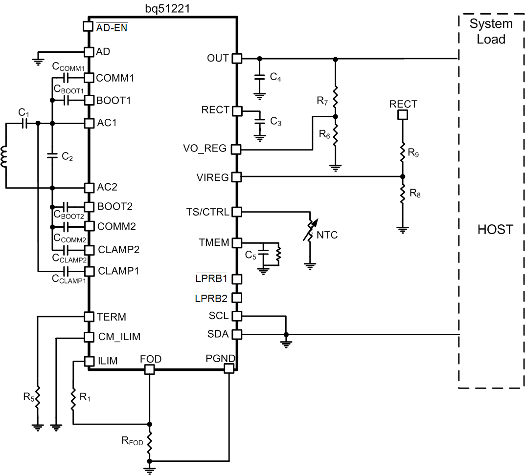
4 简化电路原理图
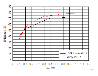
bq51221 双路模式效率 5V 输出