ZHCSF53A April 2016 – June 2016
PRODUCTION DATA.
- 1 特性
- 2 应用
- 3 说明
- 4 修订历史记录
- 5 Device Comparison
- 6 Pin Configuration and Functions
- 7 Specifications
-
8 Detailed Description
- 8.1 Overview
- 8.2 Functional Block Diagram
- 8.3
Feature Description
- 8.3.1 MP-A5 Coil Specification
- 8.3.2 High Voltage Dedicated Charging Port (HVDCP) Negotiation
- 8.3.3 Fast Charge Support
- 8.3.4 Option Select Pins
- 8.3.5 FOD and Parasitic Metal Object Detect (PMOD) Calibration
- 8.3.6 FOD Ping Calibration
- 8.3.7 Shut Down Through External Thermal Sensor or Trigger
- 8.3.8 Fault Handling and Indication
- 8.3.9 Power Transfer Start Signal
- 8.3.10 Power-On Reset
- 8.3.11 External Reset, RESET Pin
- 8.3.12 Trickle Charge and CS100
- 8.4 Device Functional Modes
- 9 Application and Implementation
- 10Power Supply Recommendations
- 11Layout
- 12器件和文档支持
- 13机械、封装和可订购信息
9 Application and Implementation
NOTE
Information in the following applications sections is not part of the TI component specification, and TI does not warrant its accuracy or completeness. TI’s customers are responsible for determining suitability of components for their purposes. Customers should validate and test their design implementation to confirm system functionality.
9.1 Application Information
The bq501210 device is a wireless power transmitter controller designed for 15-W WPC compliant applications and 5-W applications with WPC v1.1 low power receivers. It integrates all functions required to control wireless power transfer to a WPC v1.2 compliant receiver. Several tools are available for the design of the system. See the product folder (www.ti.com/product/bq501210) for more details. The following sections highlight some of the system design considerations.
9.2 Typical Application
Figure 9 shows the application block diagram for the transmitter.
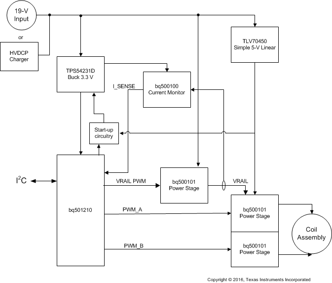 Figure 9. bq501210 System Diagram
9.2.1 Design Requirements
Table 4. Design Parameters
| DESIGN PARAMETER | VALUE |
|---|---|
| WPC coil type | MP-A5 |
| Input voltage | 15 V to 19 V provides full 15-W operation. HVDCP negotiated 9 V or 12 V provides < 15 W 5 V provides up to 4.5 W |
9.2.2 Detailed Design Procedure
9.2.2.1 Capacitor Selection
Capacitor selection is critical to proper system operation. The total capacitance value of 2 × 100 nF + 47 nF is required in the resonant tank. This is the WPC system compatibility requirement, not a guideline.
NOTE
A total capacitance value of 2 × 100 nF + 47 nF (C0G dielectric type, 100-V rating) is required in the resonant tank to achieve the correct resonance frequency.
The capacitors chosen must be rated for at least 100 V and must be of a high-quality C0G dielectric (sometimes also called NP0). These are typically available in a 5% tolerance, which is adequate. TI does not recommend the use of X7R types or below if WPC compliance is required because critical WPC Certification Testing, such as the minimum modulation or guaranteed power test, might fail.
The designer can combine capacitors to achieve the desired capacitance value. Various combinations can work depending on market availability. All capacitors must be of C0G types (not mixed with any other dielectric types).
9.2.2.2 Current Monitoring Requirements
The bq501210 is WPC v1.2 ready. To enable the PMOD or FOD features, provide current monitoring in the design.
For proper scaling of the current monitor signal, the current sense resistor should be 20 mΩ and the current shunt amplifier should have a gain of 50, such as the bq500100 (SBOS765). For FOD accuracy, the current sense resistor must be a quality component with 0.5% tolerance, at least 1/4-W rating, and a temperature stability of ±200 PPM. Proper current sensing techniques in the application hardware should also be observed.
9.2.2.3 All Unused Pins
All unused pins can be left open unless otherwise indicated. Refer to the table in Pin Configuration and Functions. To improve PCB layout, ground unused pins, if it is an option.
9.2.2.4 Input Regulators
The bq501210 requires 3.3 VDC to operate. A buck converter is used to step down from the supply voltage, such as the TPS54231D used in this design.
9.2.2.5 Input Power Requirements
The bq501210 system works with 5-V to 19-V input voltage. Levels between 15 V and 19 V will deliver 15 W, which is required for a WPC Extended Power Profile (EPP) transmitter.
5-V input supplies are aimed to negotiate to HVDCP voltages of 9 V or 12 V which enables Fast Charging of capable receivers. The system may also deliver power as a normal 5-V transmitter, however, the power level will be reduced and provinging power to higher voltage receivers may not be successful. A typical 5-V receiver has shown to produce 4.5 W consistently. Coupling and other factors will greatly influence the results of each system.
9.2.2.6 LED Mode
The bq501210 can directly drive three LED outputs (LED-A, LED-B, and LED-C). Select one of the desired LED indication schemes by choosing the selection resistor connected between LED_MODE and GND.
9.2.3 Application Curves
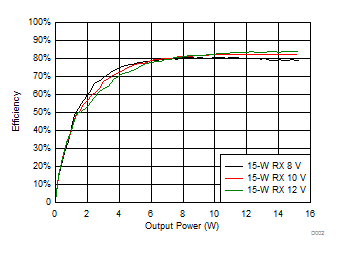
| WPC 15-W Receiver Output Voltages | ||
| 8 V, 10 V, 12 V |
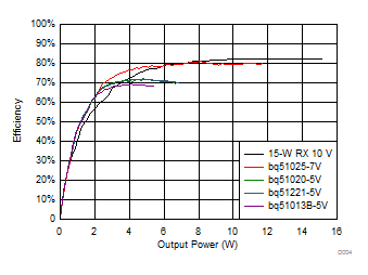
| 5-W RX (5-V Out) | bq51020, bq51221, bq51013B | |
| 10-W RX (7-V Out) | bq51025 | |
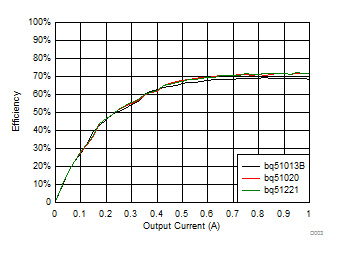
| WPC v1.1 RX (5-V Output) | ||
| bq51013B, bq51020, bq51221 |
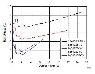
| 5-W RX (5-V Out) | bq51020, bq51221, bq51013B | |
| 10-W RX (7-V Out) | bq51025 | |