SLUSCU2 November 2017
PRODUCTION DATA.
- 1 Features
- 2 Applications
- 3 Description
- 4 Revision History
- 5 Description (Continued)
- 6 Pin Configuration and Functions
- 7 Specifications
-
8 Detailed Description
- 8.1 Overview
- 8.2 Functional Block Diagram
- 8.3 Feature Description
- 8.4 Device Functional Modes
- 8.5 Programming
- 8.6
Register Map
- 8.6.1
Setting Charge and PROCHOT Options
- 8.6.1.1 ChargeOption0 Register (SMBus address = 12h) [reset = E20Eh]
- 8.6.1.2 ChargeOption1 Register (SMBus address = 30h) [reset = 211h]
- 8.6.1.3 ChargeOption2 Register (SMBus address = 31h) [reset = 2B7]
- 8.6.1.4 ChargeOption3 Register (SMBus address = 32h) [reset = 0h]
- 8.6.1.5 ProchotOption0 Register (SMBus address = 33h) [reset = 04A54h]
- 8.6.1.6 ProchotOption1 Register (SMBus address = 34h) [reset = 8120h]
- 8.6.1.7 ADCOption Register (SMBus address = 35h) [reset = 2000h]
- 8.6.2 Charge and PROCHOT Status
- 8.6.3 ChargeCurrent Register (SMBus address = 14h) [reset = 0h]
- 8.6.4 MaxChargeVoltage Register (SMBus address = 15h) [reset value based on CELL_BATPRESZ pin setting]
- 8.6.5 MinSystemVoltage Register (SMBus address = 3Eh) [reset value based on CELL_BATPRESZ pin setting]
- 8.6.6 Input Current and Input Voltage Registers for Dynamic Power Management
- 8.6.7 ADCVBUS/PSYS Register (SMBus address = 23h)
- 8.6.8 ADCIBAT Register (SMBus address = 24h)
- 8.6.9 ADCIINCMPIN Register (SMBus address = 25h)
- 8.6.10 ADCVSYSVBAT Register (SMBus address = 26h) (reset = )
- 8.6.11 ID Registers
- 8.6.1
Setting Charge and PROCHOT Options
- 9 Application and Implementation
- 10Power Supply Recommendations
- 11Layout
- 12Device and Documentation Support
- 13Mechanical, Packaging, and Orderable Information
1 Features
- Charge 1- to 4-Cell Battery From Wide Range of Input Sources
- 3.5-V to 24-V Input Operating Voltage
- Supports USB2.0, USB 3.0, USB 3.1 (Type C), and USB_PD Input Current Settings
- Seamless Transition Between Buck and Boost Operation
- Input current and Voltage Regulation (IDPM and VDPM) Against Source Overload
- Power/Current Monitor for CPU Throttling
- Comprehensive PROCHOT Profile, IMVP8 Compliant
- Input and Battery Current Monitor
- System Power Monitor, IMVP8 Compliant
- Narrow-VDC (NVDC) Power Path Management
- Instant-On With No Battery or Deeply Discharged Battery
- Battery Supplements System When Adapter is Fully-Loaded
- Ideal Diode Operation in Supplement Mode
- 800-kHz or 1.2-MHz Programmable Switching Frequency for 1-µH to 3.3-µH Inductor
- Host Control Interface for Flexible System Configuration
- SMBus Port for Optimal System Performance and Status Reporting
- Hardware Pin to Set Input Current Limit Without EC Control
- Integrated ADC to Monitor Voltage, Current and Power
- High Accuracy Regulation and Monitor
- ±0.5% Charge Voltage Regulation
- ±2% Input/Charge Current Regulation
- ±2% Input/Charge Current Monitor
- ±5% Power Monitor
- Safety
- Thermal Shutdown
- Input, System, Battery Overvoltage Protection
- MOSFET Inductor Overcurrent Protection
- Low Battery Quiescent Current
- Input Current Optimizer (ICO) to Extract Max Input Power
- Charge any Battery Chemistry: Li+, LiFePO4, NiCd, NiMH, Lead Acid
- Package: 32-Pin 4 × 4 WQFN
2 Applications
- Ultra-Books, Notebooks, Detachable, and Tablet PCs and Power Bank
- Industrial and Medical Equipment
- Portable Equipment With Rechargeable Batteries
3 Description
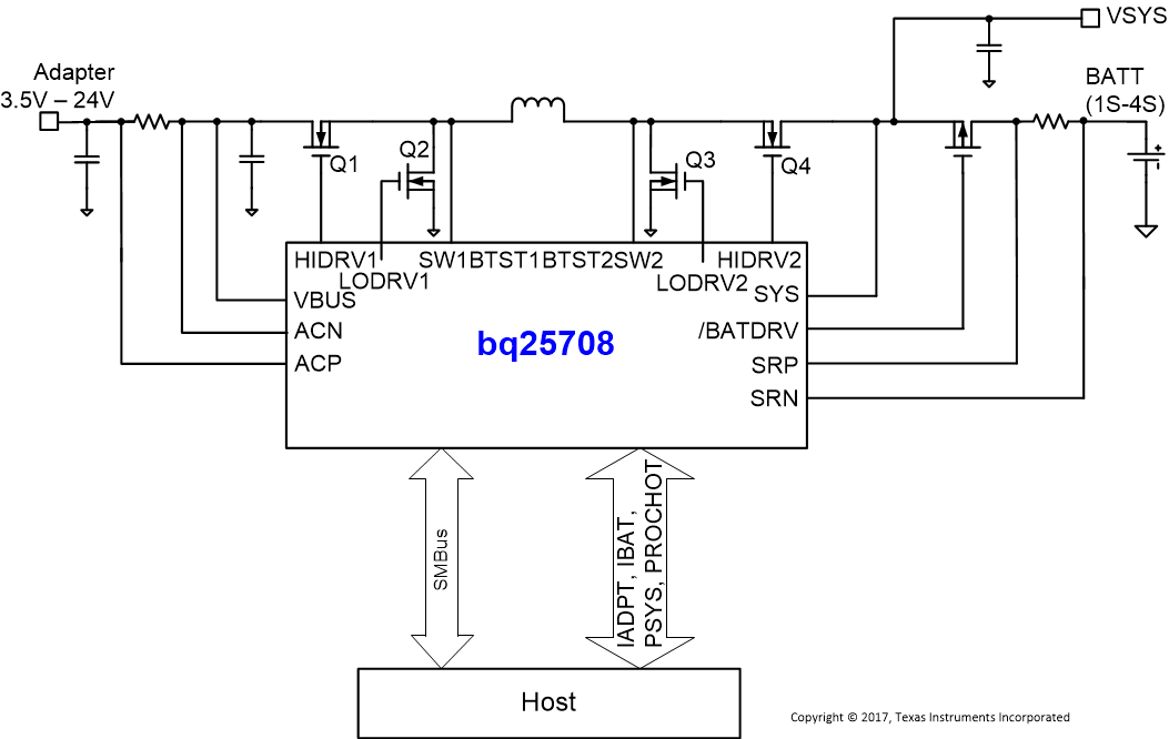
The bq25708 is a synchronous NVDC battery buck-boost charge controller, offering low component count, high efficiency solution for space-constraint, multi-chemistry battery charging applications.
The NVDC-1 configuration allows the system to be regulated at battery voltage, but not drop below system minimum voltage. The system keeps operating even when the battery is completely discharged or removed. When load power exceeds input source rating, the battery goes into supplement mode and prevents the system from crashing.
The bq25708 charges battery from a wide range of input sources including USB adapter, high voltage USB PD sources and traditional adapters.
Device Information (1)
| PART NUMBER | PACKAGE | BODY SIZE (NOM) |
|---|---|---|
| bq25708 | WQFN (32) | 4.00 mm × 4.00 mm |
- For all available packages, see the orderable addendum at the end of the data sheet.
Application Diagram
