ZHCSGR7 September 2017
PRODUCTION DATA.
- 1 特性
- 2 应用
- 3 说明
- 4 修订历史记录
- 5 说明 (续)
- 6 Pin Configuration and Functions
- 7 Specifications
-
8 Detailed Description
- 8.1 Overview
- 8.2 Functional Block Diagram
- 8.3
Feature Description
- 8.3.1 Power-On-Reset (POR)
- 8.3.2 Device Power Up from Battery without Input Source
- 8.3.3 Power Up from Input Source
- 8.3.4 Host Mode and Standalone Power Management
- 8.3.5 Power Path Management
- 8.3.6 Battery Charging Management
- 8.3.7 Shipping Mode
- 8.3.8 Status Outputs (PG, STAT)
- 8.3.9 Protections
- 8.3.10 Serial interface
- 8.4 Register Maps
- 9 Application and Implementation
- 10Power Supply Recommendations
- 11Layout
- 12器件和文档支持
- 13机械、封装和可订购信息
9 Application and Implementation
NOTE
information in the following applications sections is not part of the TI component specification, and TI does not warrant its accuracy or completeness. TI’s customers are responsible for determining suitability of components for their purposes. Customers should validate and test their design implementation to confirm system functionality.
9.1 Application information
A typical application consists of the device configured as an I2C controlled parallel charger with a main charger bq25600 to fast charge single cell Li-Ion and Li-polymer batteries used in a wide range of smart phones and other portable devices. bq25600 and bq25660C have different I2C address so that two devices can share the same I2C bus.
9.2 Typical Application Diagram
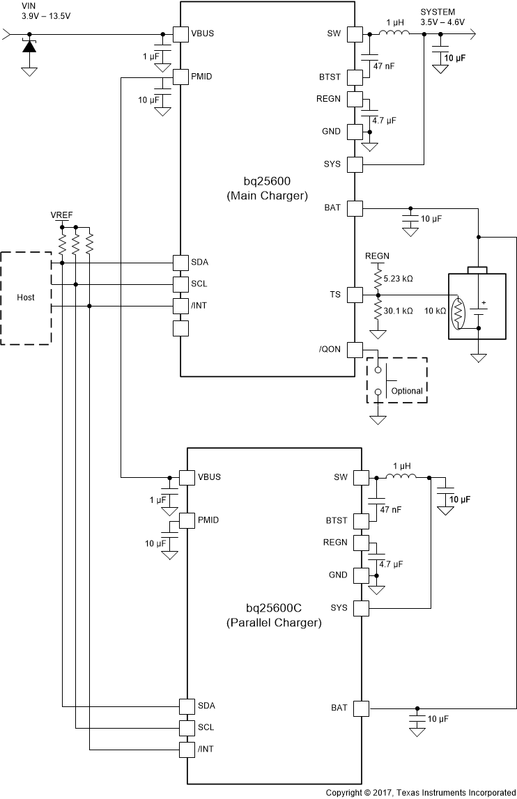 Figure 19. Parallel Charger Application
9.2.1 Design Requirements
9.2.2 Detailed Design Procedure
9.2.2.1 Inductor Selection
The 1.5-MHz switching frequency allows the use of small inductor and capacitor values to maintain an inductor saturation current higher than the charging current (ICHG) plus half the ripple current (IRIPPLE):
The inductor ripple current depends on the input voltage (VVBUS), the duty cycle (D = VBAT/VVBUS), the switching frequency (fS) and the inductance (L).

The maximum inductor ripple current occurs when the duty cycle (D) is 0.5 or approximately 0.5. Usually inductor ripple is designed in the range between 20% and 40% maximum charging current as a trade-off between inductor size and efficiency for a practical design.
9.2.2.2 input Capacitor
Design input capacitance to provide enough ripple current rating to absorb input switching ripple current. The worst case RMS ripple current is half of the charging current when duty cycle is 0.5. If the converter does not operate at 50% duty cycle, then the worst case capacitor RMS current ICin occurs where the duty cycle is closest to 50% and can be estimated using Equation 3.

Low ESR ceramic capacitor such as X7R or X5R is preferred for input decoupling capacitor and should be placed to the drain of the high-side MOSFET and source of the low-side MOSFET as close as possible. Voltage rating of the capacitor must be higher than normal input voltage level. A rating of 25-V or higher capacitor is preferred for 15 V input voltage. Capacitance of 22-μF is suggested for typical of 3A charging current.
9.2.2.3 Output Capacitor
Ensure that the output capacitance has enough ripple current rating to absorb the output switching ripple current. Equation 4 shows the output capacitor RMS current ICOUT calculation.

The output capacitor voltage ripple can be calculated as follows:

At certain input and output voltage and switching frequency, the voltage ripple can be reduced by increasing the output filter LC.
The charger device has internal loop compensation optimized for >20μF ceramic output capacitance. The preferred ceramic capacitor is 10V rating, X7R or X5R.
9.3 Application Curves
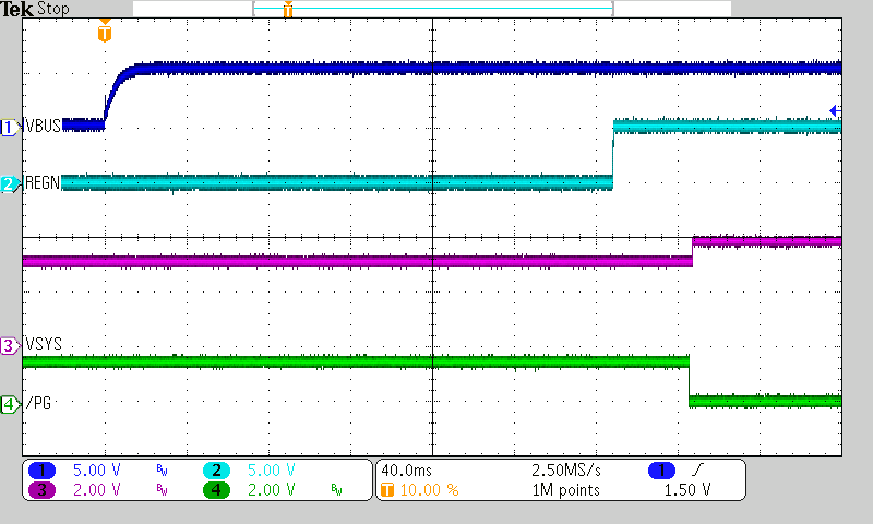
| VVBUS = 5 V | VVBAT = 3.2 V |
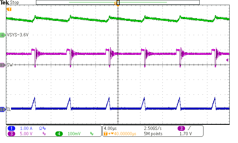
| VVBUS = 5 V | |
| ISYS = 50 mA | Charge Disabled |
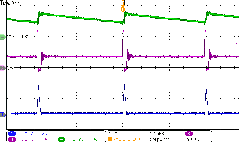
| VVBUS = 12 V | |
| ISYS = 50 mA | Charge Disabled |
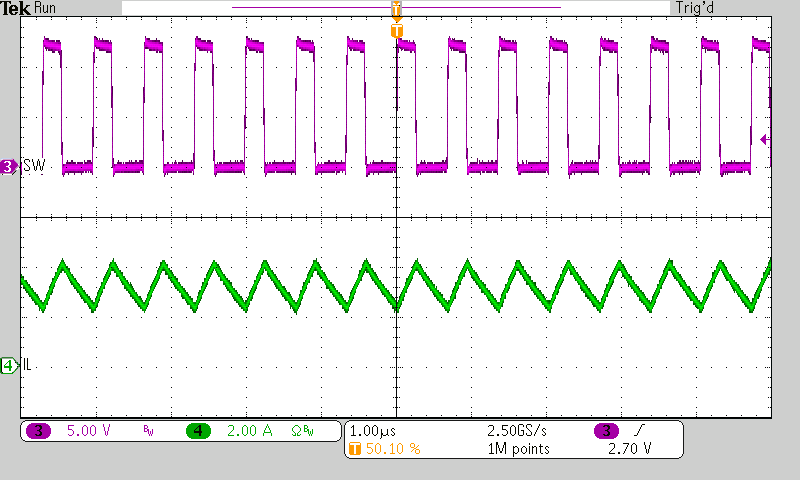
| VVBUS = 12 V | VVBAT = 3.8 V |
| ICHG = 2 A |
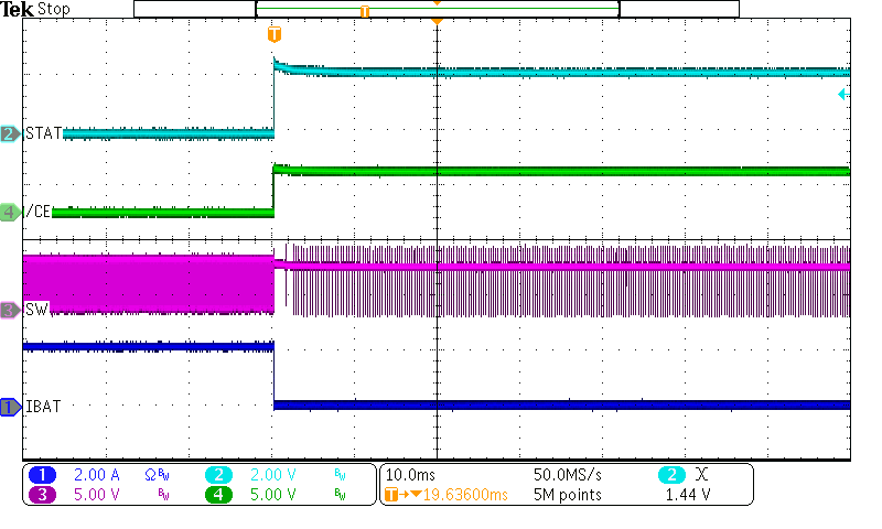
| VVBUS = 5 V | VVBAT = 3.2 V |
| ICHG = 2 A |
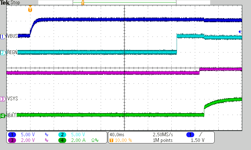
| VVBUS = 5 V | VVBAT = 3.2 V |
| ICHG = 2 A |
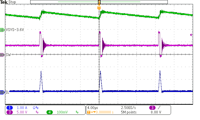
| VVBUS = 9 V | |
| ISYS = 50 mA | Charge Disabled |
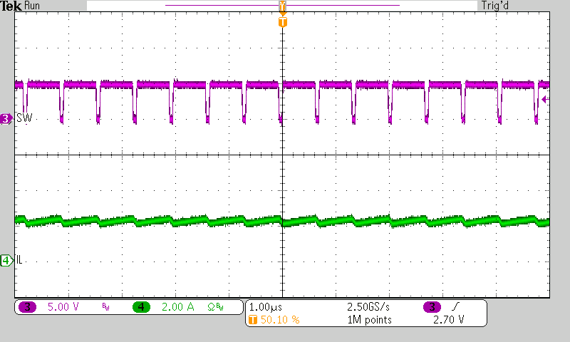
| VVBUS = 5 V | VVBAT = 3.8 V |
| ICHG = 2 A |
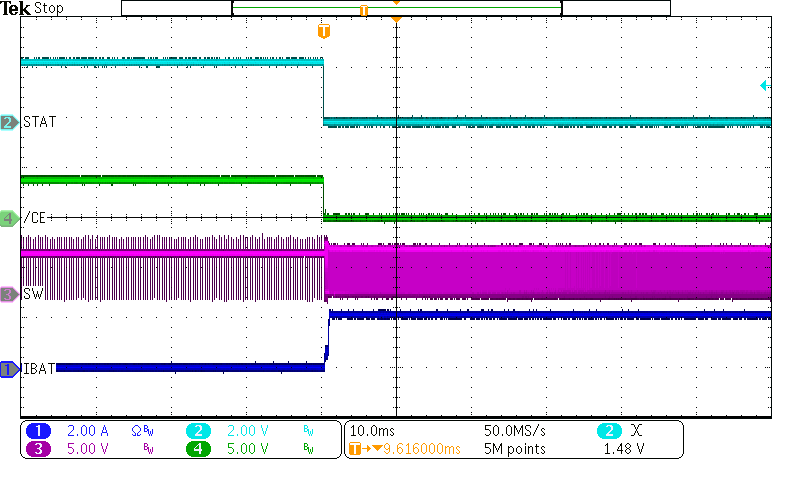
| VVBUS = 5 V | VVBAT = 3.2 V |
| ICHG = 2 A |