ZHCSDP2B May 2015 – June 2017
UNLESS OTHERWISE NOTED, this document contains PRODUCTION DATA.
- 1 特性
- 2 应用
- 3 说明
- 4 修订历史记录
- 5 Pin Configuration and Functions
- 6 Specifications
-
7 Detailed Description
- 7.1 Overview
- 7.2 Functional Block Diagram
- 7.3
Feature Description
- 7.3.1 Battery Preconditioning
- 7.3.2 Battery Fast-Charge Constant Current
- 7.3.3 Charge-Current Monitor
- 7.3.4 Battery Fast-Charge Voltage Regulation
- 7.3.5 Charge Termination Detection and Recharge
- 7.3.6 Charge Status Outputs
- 7.3.7 PG Output (bq24080-Q1)
- 7.3.8 Charge-Enabled (CE) Input (bq24080-Q1)
- 7.3.9 Timer Enabled (TE) Input (bq24081-Q1)
- 7.3.10 Temperature Qualification (bq24081-Q1)
- 7.3.11 Timer Fault and Recovery
- 7.4 Device Functional Modes
- 8 Application and Implementation
- 9 Power Supply Recommendations
- 10Layout
- 11器件和文档支持
- 12机械、封装和可订购信息
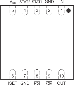
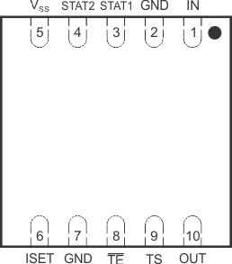
5 Pin Configuration and Functions
bq24080-Q1 DRC Package
10 Pin VSON
Top View

bq24081-Q1 DRC Package
10 Pin VSON
Top View

Pin Functions
| PIN | I/O | DESCRIPTION | ||
|---|---|---|---|---|
| NAME | NO. | |||
| bq24080-Q1 | bq24081-Q1 | |||
| CE | 9 | – | I | Charge enable input (active-low) |
| GND | 2, 7 | 2, 7 | – | Ground |
| IN | 1 | 1 | I | Adapter dc voltage. Connect minimum 0.1-μF capacitor to VSS. |
| ISET | 6 | 6 | I | Charge current. External resistor to VSS sets precharge and fast-charge current, and also the termination current value. Can be used to monitor the charge current. |
| OUT | 10 | 10 | O | Charge current output. Connect minimum 0.1-μF capacitor to VSS. |
| PG | 8 | – | O | Power-good status output (open-drain) |
| STAT1 | 3 | 3 | O | Charge status outputs (open-drain) |
| STAT2 | 4 | 4 | O | |
| TE | – | 8 | I | Timer-enable input (active-low) |
| TS | – | 9 | I/O | Temperature sense; connect to NTC in battery pack. |
| VSS | 5 | 5 | – | Ground |
| Thermal pad | – | – | – | There is an internal electrical connection between the exposed thermal pad and the VSS pin of the device. The exposed thermal pad must be connected to the same potential as the VSS pin on the printed-circuit board. Do not use the thermal pad as the primary ground input for the device. The VSS pin must be connected to ground at all times. |