ZHCSES2H December 2009 – February 2016 ADS1282-HT
PRODUCTION DATA.
- 1 特性
- 2 应用
- 3 说明
- 4 修订历史记录
- 5 说明 (续)
- 6 Pin Configuration and Functions
-
7 Specifications
- 7.1 Absolute Maximum Ratings
- 7.2 Recommended Operating Conditions
- 7.3 Thermal Information
- 7.4 Electrical Characteristics
- 7.5 Electrical Characteristics (PW Package)
- 7.6 Timing Requirements
- 7.7 Pulse-Sync Timing Requirements
- 7.8 Reset Timing Requirements
- 7.9 Switching Characteristics
- 7.10 Modulator Switching Characteristics
- 7.11 Typical Characteristics
-
8 Detailed Description
- 8.1 Overview
- 8.2 Functional Block Diagram
- 8.3
Feature Description
- 8.3.1 Noise Performance
- 8.3.2 Input-Referred Noise
- 8.3.3 Idle Tones
- 8.3.4 Operating Mode
- 8.3.5 Analog Inputs and Multiplexer
- 8.3.6 PGA (Programmable Gain Amplifier)
- 8.3.7 ADC
- 8.3.8 Modulator
- 8.3.9 Modulator Over-Range
- 8.3.10 Modulator Input Impedance
- 8.3.11 Modulator Over-Range Detection (MFLAG)
- 8.3.12 Voltage Reference Inputs (VREFP, VREFN)
- 8.3.13 Digital Filter
- 8.3.14 Master Clock Input (CLK)
- 8.3.15 Synchronization (SYNC Pin and Sync Command)
- 8.3.16 Pulse-Sync Mode
- 8.3.17 Continuous-Sync Mode
- 8.3.18 Reset (RESET Pin and Reset Command)
- 8.3.19 Power-Down (PWDN Pin and Standby Command)
- 8.3.20 Power-On Sequence
- 8.3.21 Serial Interface
- 8.3.22 Data Format
- 8.3.23 Reading Data
- 8.3.24 One-Shot Operation
- 8.4 Device Functional Modes
- 8.5
Programming
- 8.5.1
Commands
- 8.5.1.1 WAKEUP: Wake-Up from Standby Mode
- 8.5.1.2 STANDBY: Standby Mode
- 8.5.1.3 SYNC: Synchronize the A/D Conversion
- 8.5.1.4 RESET: Reset the Device
- 8.5.1.5 RDATAC: Read Data Continuous
- 8.5.1.6 SDATAC: Stop Read Data Continuous
- 8.5.1.7 RDATA: Read Data By Command
- 8.5.1.8 RREG: Read Register Data
- 8.5.1.9 WREG: Write to Register
- 8.5.1.10 OFSCAL: Offset Calibration
- 8.5.1.11 GANCAL: Gain Calibration
- 8.5.2 Calibration Commands
- 8.5.3 User Calibration
- 8.5.4 Configuration Guide
- 8.5.1
Commands
- 8.6 Register Maps
- 9 Application and Implementation
- 10Power Supply Recommendations
- 11器件和文档支持
- 12机械、封装和可订购信息
封装选项
机械数据 (封装 | 引脚)
散热焊盘机械数据 (封装 | 引脚)
- PW|28
订购信息
8 Detailed Description
8.1 Overview
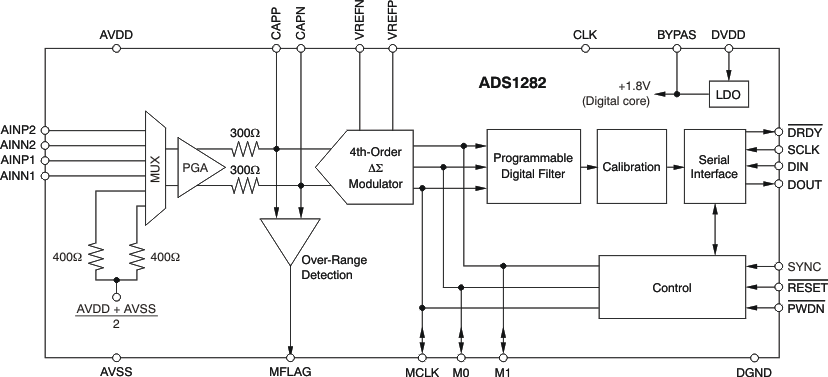
The ADS1282-HT is a high-performance analog-to-digital converter (ADC) intended for energy exploration, seismic monitoring, chromatography, and other exacting applications. The converter provides 24- or 32-bit output data in data rates from 250 SPS to 4000 SPS. The Functional Block Diagram shows the block diagram of the ADS1282-HT.
The two-channel input MUX allows five configurations: Input 1; Input 2; Input 1 and Input 2 shorted together; shorted with 400-Ω test; and common-mode test. The input MUX is followed by a continuous time PGA, featuring very low noise of 5 nV/√Hz. The PGA is controlled by register settings, allowing gains of 1 to 64.
The inherently-stable, fourth-order, delta-sigma modulator measures the differential input signal VIN = (AINP – AINN) × PGA against the differential reference VREF = (VREFP – VREFN). A digital output (MFLAG) indicates that the modulator is in overload as a result of an overdrive condition. The modulator output is available directly on the MCLK, M0, and M1 output pins when in modulator mode. The modulator connects to an on-chip digital filter that provides the output code readings.
The digital filter consists of a variable decimation rate, fifth-order sinc filter followed by a variable phase, decimate-by-32, finite-impulse response (FIR) low-pass filter with programmable phase, and then by an adjustable high-pass filter for DC removal of the output reading. The output of the digital filter can be taken from the sinc, the FIR low-pass, or the infinite impulse response (IIR) high-pass sections.
Gain and offset registers scale the digital filter output to produce the final code value. The scaling feature can be used for calibration and sensor gain matching. The output data word is provided as either a 24-bit word or a full 32-bit word, allowing complete utilization of the inherently high resolution.
The SYNC input resets the operation of both the digital filter and the modulator, allowing synchronization conversions of multiple ADS1282-HT devices to an external event. The SYNC input supports a continuously-toggled input mode that accepts an external data frame clock locked to the conversion rate.
The RESET input resets the register settings and also restarts the conversion process. The PWDN input sets the device into a micro-power state. The register settings are not retained in PWDN mode. Use the STANDBY command in its place if it is desired to retain register settings (the quiescent current in the Standby mode is slightly higher).
Noise-immune Schmitt-trigger and clock-qualified inputs (RESET and SYNC) provide increased reliability in high-noise environments. The serial interface is used to read conversion data, in addition to reading from and writing to the configuration registers.
The device features unipolar and bipolar analog power supplies (AVDD and AVSS, respectively) for input range flexibility and a digital supply accepting 1.8 V to 3.3 V. The analog supplies may be set to 5 V to accept unipolar signals (with input offset) or set lower in the range of ±2.5 V to accept true bipolar input signals (ground referenced).
An internal sub-regulator is used to supply the digital core from DVDD. The BYPAS pin (pin 28) is the sub-regulator output and requires a 1-μF capacitor for noise reduction. BYPAS should not be used to drive external circuitry.
8.2 Functional Block Diagram
8.3 Feature Description
8.3.1 Noise Performance
The ADS1282-HT device offers outstanding noise performance (SNR). SNR depends on the data rate, the PGA setting, and the mode. As the bandwidth is reduced by decreasing the data rate, the SNR improves correspondingly. Similarly, as the PGA gain is increased, the SNR decreases. Table 1 summarizes the noise performance versus data rate, PGA setting, and mode.
8.3.2 Input-Referred Noise
The input-referred noise is related to SNR by Equation 1:

where
- FSRRMS = Full-scale range RMS = (VREFP – VREFN)/(2 × √2 × PGA)
- NRMS = Noise RMS (input-referred)
8.3.3 Idle Tones
The ADS1282-HT modulator incorporates an internal dither signal that randomizes the idle tone energy. Low-level idle tones may still be present, typically –137-dB less than full-scale. The low-level idle tones can be shifted out of the passband with an external offset = 20 mV/PGA. See the Application Information section for the recommended offset circuit.
8.3.4 Operating Mode
The default mode is high-resolution.
Table 1. Signal-to-Noise Ratio (dB)(1)
| DATA RATE (SPS) | PGA | ||||||
|---|---|---|---|---|---|---|---|
| 1 | 2 | 4 | 8 | 16 | 32 | 64 | |
| 250 | 130 | 130 | 129 | 128 | 125 | 119 | 114 |
| 500 | 127 | 127 | 126 | 125 | 122 | 116 | 111 |
| 1000 | 124 | 124 | 123 | 122 | 119 | 113 | 108 |
| 2000 | 121 | 121 | 120 | 119 | 116 | 111 | 106 |
| 4000 | 118 | 118 | 117 | 116 | 113 | 108 | 103 |
8.3.5 Analog Inputs and Multiplexer
Figure 26 shows a diagram of the input multiplexer.
ESD diodes protect the multiplexer inputs. If either input is taken less than AVSS – 0.3 V or greater than AVDD + 0.3 V, the ESD protection diodes may turn on. If these conditions are possible, external Schottky clamp diodes and/or series resistors may be required to limit the input current to safe values (see the Absolute Maximum Ratings).
Also, overdriving one unused input may affect the conversions of the other input. If overdriven inputs are possible, TI recommends clamping the signal with external Schottky diodes.
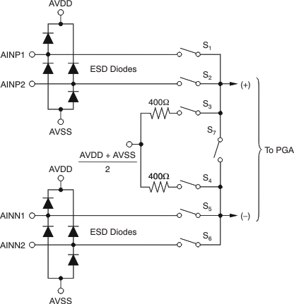 Figure 26. Analog Inputs and Multiplexer
The specified input operating range of the PGA is shown in Equation 2:
Absolute input levels (input signal level and common-mode level) should be maintained within these limits for best operation.
The multiplexer connects one of the two external differential inputs to the preamplifier inputs, in addition to internal connections for various self-test modes. Table 2 summarizes the multiplexer configurations for Figure 26.
Table 2. Multiplexer Modes
| MUX[2:0] | SWITCHES | DESCRIPTION |
|---|---|---|
| 000 | S1, S5 | AINP1 and AINN1 connected to preamplifier |
| 001 | S2, S6 | AINP2 and AINN2 connected to preamplifier |
| 010 | S3, S4 | Preamplifier inputs shorted together through 400Ω internal resistors |
| 011 | S1, S5, S2, S6 | AINP1, AINN1 and AINP2, AINN2 connected together and to the preamplifier |
| 100 | S6, S7 | External short, preamplifier inputs shorted to AINN2 (common-mode test) |
The typical on-resistance (RON) of the multiplexer switch is 30 Ω. When the multiplexer is used to drive an external load on one input by a signal generator on the other input, on-resistance and on-resistance amplitude dependency can lead to measurement errors. Figure 27 shows THD versus load resistance and amplitude. THD improves with high-impedance loads and with lower amplitude drive signals. The data are measured with the circuit from Figure 28 with MUX[2:0] = 011.
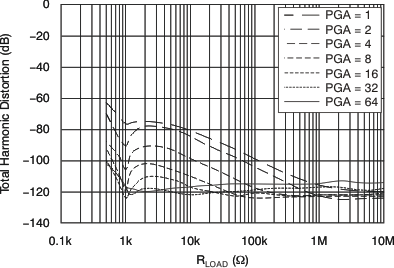 Figure 27. THD vs External Load and Signal Magnitude (PGA) (See Figure 28)
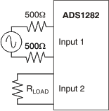 Figure 28. Driving an External Load Through the MUX
8.3.6 PGA (Programmable Gain Amplifier)
The PGA of the ADS1282-HT is a low-noise, continuous-time, differential-in/differential-out CMOS amplifier. The gain is programmable from 1 to 64, set by register bits, PGA[2:0]. The PGA differentially drives the modulator through 300-Ω internal resistors. A COG capacitor (10 nF typical) must be connected to CAPP and CAPN to filter modulator sampling glitches. The external capacitor also serves as an anti-alias filter. The corner frequency is given in Equation 3:

Referring to Figure 29, amplifiers A1 and A2 are chopped to remove the offset, offset drift, and the 1/f noise. Chopping moves the effects to ƒCLK/128 (8 kHz), which is safely out of the passband. Chopping can be disabled by setting the CHOP register bit = 0. With chopping disabled, the impedance of the PGA increases substantially (>> 1 GΩ). As shown in Figure 30, chopping maintains flat noise density; if chopping is disabled, however, it results in a rising 1/f noise profile.
The PGA has programmable gains from 1 to 64. Table 3 shows the register bit setting for the PGA and resulting full-scale differential range.
The specified output operating range of the PGA is shown in Equation 4:
PGA output levels (signal plus common-mode) should be maintained within these limits for best operation.
Table 3. PGA Gain Settings
| PGA[2:0] | GAIN | DIFFERENTIAL INPUT RANGE (V)(1) |
|---|---|---|
| 000 | 1 | ±2.5 |
| 001 | 2 | ±1.25 |
| 010 | 4 | ±0.625 |
| 011 | 8 | ±0.312 |
| 100 | 16 | ±0.156 |
| 101 | 32 | ±0.078 |
| 110 | 64 | ±0.039 |
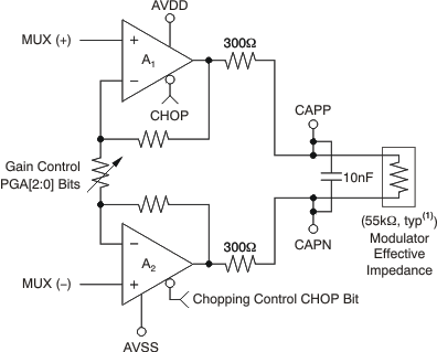 Figure 29. PGA Block Diagram
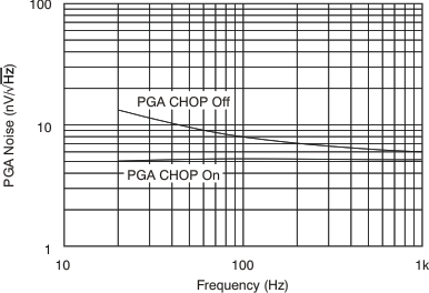 Figure 30. PGA Noise
8.3.7 ADC
The ADC block of the ADS1282-HT is composed of two sections: a high-accuracy modulator and a programmable digital filter.
8.3.8 Modulator
The high-performance modulator is an inherently-stable, fourth-order, ΔΣ, 2 + 2 pipelined structure, as Figure 31 shows. It shifts the quantization noise to a higher frequency (out of the passband) where digital filtering can easily remove it. The modulator can be filtered either by the on-chip digital filter or by use of post-processing filters.
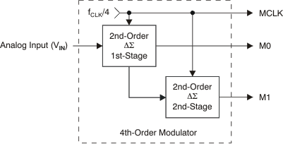 Figure 31. Fourth-Order Modulator
The modulator first stage converts the analog input voltage into a pulse-code modulated (PCM) stream. When the level of differential analog input (AINP – AINN) is near one-half the level of the reference voltage 1/2 × (VREFP – VREFN), the ‘1’ density of the PCM data stream is at its highest. When the level of the differential analog input is near zero, the PCM ‘0’ and ‘1’ densities are nearly equal. At the two extremes of the analog input levels (+FS and –FS), the ‘1’ density of the PCM streams is approximately 90% and 10%, respectively.
The modulator second stage produces a '1' density data stream designed to cancel the quantization noise of the first stage. The data streams of the two stages are then combined before the digital filter stage, as shown in Equation 5.
M0[n] represents the most recent first-stage output while M0[n – 1] is the previous first-stage output. When the modulator output is enabled, the digital filter shuts down to save power.
The modulator is optimized for input signals within a 4-kHz passband. As Figure 32 shows, the noise shaping of the modulator results in a sharp increase in noise greater than 6 kHz. The modulator has a chopped input structure that further reduces noise within the passband. The noise moves out of the passband and appears at the chopping frequency (ƒCLK / 512 = 8 kHz). The component at 5.8 kHz is the tone frequency, shifted out of band by an external 20 mV/PGA offset. The frequency of the tone is proportional to the applied DC input and is given by PGA × VIN/0.003 (in kHz).
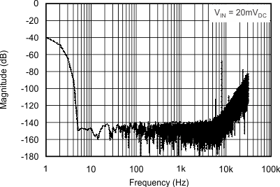
| 1-Hz resolution |
8.3.9 Modulator Over-Range
The ADS1282-HT modulator is inherently stable, and therefore, has predictable recovery behavior resulting from an input overdrive condition. The modulator does not exhibit self-resetting behavior, which often results in an unstable output data stream.
The ADS1282-HT modulator outputs a 1s density data stream at 90% duty cycle with the positive full-scale input signal applied (10% duty cycle with the negative full-scale signal). If the input is overdriven past 90% modulation, but less than 100% modulation (10% and 0% for negative overdrive, respectively), the modulator remains stable and continues to output the 1s density data stream. The digital filter may or may not clip the output codes to +FS or –FS, depending on the duration of the overdrive. When the input returns to the normal range from a long duration overdrive (worst case), the modulator returns immediately to the normal range, but the group delay of the digital filter delays the return of the conversion result to within the linear range (31 readings for linear phase FIR). 31 additional readings (62 total) are required for completely settled data.
If the inputs are sufficiently overdriven to drive the modulator to full duty cycle, all 1s or all 0s, the modulator enters a stable saturated state. The digital output code may clip to +FS or –FS, again depending on the duration. A small duration overdrive may not always clip the output code. When the input returns to the normal range, the modulator requires up to 12 modulator clock cycles (ƒMOD) to exit saturation and return to the linear region. The digital filter requires an additional 62 conversions for fully settled data (linear phase FIR).
In the extreme case of over-range, either input is overdriven, exceeding the voltage of either analog supply voltage plus an internal ESD diode drop. The internal diodes begin to conduct and the signal on the input is clipped. When the input overdrive is removed, the diodes recover quickly. Keep in mind that the input current must be limited to 100-mA peak or 10-mA continuous if an overvoltage condition is possible.
8.3.10 Modulator Input Impedance
The modulator samples the buffered input voltage with an internal capacitor to perform conversions. The charging of the input sampling capacitor draws a transient current from the PGA output. The average value of the current can be used to calculate an effective input impedance of:
where
- ƒMOD = Modulator sample frequency, Mode = CLK / 4
- CS = Input sampling capacitor (17 pF, typ)
The resulting modulator input impedance for CLK = 4.096 MHz is 55 kΩ. The modulator input impedance and the PGA output resistors result in a systematic gain error of –1%. CS can vary ±20% over production lots, affecting the gain error.
8.3.11 Modulator Over-Range Detection (MFLAG)
The ADS1282-HT has a fast-responding over-range detection that indicates when the differential input exceeds ±100% full scale. The threshold tolerance is ±2.5%.The MFLAG output asserts high when in an over-range condition. As Figure 33 and Figure 34 illustrate, the absolute differential input is compared to 100% of range. The output of the comparator is sampled at the rate of ƒMOD / 2, yielding the MFLAG output. The minimum MFLAG pulse width is ƒMOD / 2.
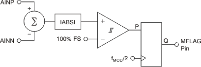 Figure 33. Modulator Over-Range Block Diagram
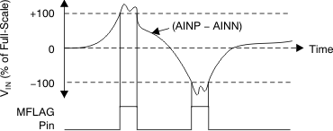 Figure 34. Modulator Over-Range Flag Operation
8.3.12 Voltage Reference Inputs (VREFP, VREFN)
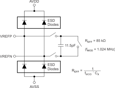
The voltage reference for the ADS1282-HT is the differential voltage between VREFP and VREFN: VREF = VREFP – VREFN. The reference inputs use a structure similar to that of the analog inputs with the circuitry of the reference inputs shown in Figure 35. The average load presented by the switched capacitor reference input can be modeled with an effective differential impedance of REFF = tSAMPLE / CIN (tSAMPLE = 1/ƒMOD). The effective impedance of the reference inputs loads the external reference.
The ADS1282-HT reference inputs are protected by ESD diodes. In order to prevent these diodes from turning on, the voltage on either input must stay within the range shown in Equation 7:
The minimum valid input for VREFN is AVSS – 0.1 V and maximum valid input for VREFP is AVDD + 0.1 V.
A high-quality 5 V reference voltage is necessary for achieving the best performance from the ADS1282-HT. Noise and drift on the reference degrade overall system performance, and it is critical that special care be given to the circuitry generating the reference voltages in order to achieve full performance. See Application Information for reference recommendations.
8.3.13 Digital Filter
The digital filter receives the modulator output and decimates the data stream. By adjusting the amount of filtering, tradeoffs can be made between resolution and data rate: filter more for higher resolution, filter less for higher data rate.
The digital filter is comprised of three cascaded filter stages: a variable-decimation, fifth-order sinc filter; a fixed-decimation FIR, low-pass filter (LPF) with selectable phase; and a programmable, first-order, high-pass filter (HPF), as shown in Figure 36.
The output can be taken from one of the three filter blocks, as Figure 36 shows. To implement the digital filter completely off-chip, select the filter bypass setting (modulator output). For partial filtering by the ADS1282-HT, select the sinc filter output. For complete on-chip filtering, activate both the sinc and FIR stages. The HPF can then be included to remove DC and low frequencies from the data. Table 4 shows the filter options.
Table 4. Digital Filter Selection
| FILTR[1:0] BITS | DIGITAL FILTERS SELECTED |
|---|---|
| 00 | Bypass; modulator output mode |
| 01 | Sinc |
| 10 | Sinc + FIR |
| 11 | Sinc + FIR + HPF (low-pass and high-pass) |
8.3.13.1 Sinc Filter Stage (Sinx/X)
The sinc filter is a variable decimation rate, fifth-order, low-pass filter. Data are supplied to this section of the filter from the modulator at the rate of ƒMOD (ƒCLK/4). The sinc filter attenuates the high-frequency noise of the modulator, then decimates the data stream into parallel data. The decimation rate affects the overall data rate of the converter; it is set by the DR[2:0] register bits, as shown in Table 5.
Equation 8 shows the scaled Z-domain transfer function of the sinc filter.

Table 5. Sinc Filter Data Rates (Clk = 4.096 MHz)
| DR[2:0] REGISTER | DECIMATION RATIO (N) | SINC DATA RATE (SPS) |
|---|---|---|
| 000 | 128 | 8000 |
| 001 | 64 | 16000 |
| 010 | 32 | 32000 |
| 011 | 16 | 64000 |
| 100 | 8 | 128000 |
Equation 9 shows the frequency domain transfer function of the sinc filter.
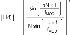
where
- N = Decimation ratio (see Table 5)
The sinc filter has notches (or zeroes) that occur at the output data rate and multiples thereof. At these frequencies, the filter has zero gain. Figure 37 shows the frequency response of the sinc filter and Figure 38 shows the roll-off of the sinc filter.
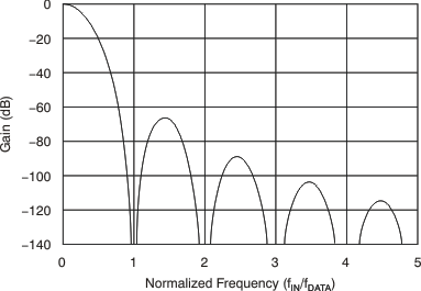 Figure 37. Sinc Filter Frequency Response
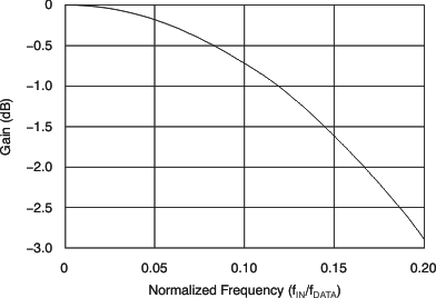 Figure 38. Sinc Filter Roll-Off
8.3.13.2 FIR Stage
The second stage of the ADS1282-HT digital filter is an FIR low-pass filter. Data are supplied to this stage from the sinc filter. The FIR stage is segmented into four sub-stages, as shown in Figure 39. The first two sub-stages are half-band filters with decimation ratios of 2. The third sub-stage decimates by 4 and the fourth sub-stage decimates by 2. The overall decimation of the FIR stage is 32. Two coefficient sets are used for the third and fourth sections, depending on the phase selection. Table 19 (in 器件支持) lists the FIR stage coefficients. Table 6 lists the data rates and overall decimation ratio of the FIR stage.
Table 6. Fir Filter Data Rates
| DR[2:0] REGISTER | DECIMATION RATIO (N) | FIR DATA RATE (SPS) |
|---|---|---|
| 000 | 4096 | 250 |
| 001 | 2048 | 500 |
| 010 | 1024 | 1000 |
| 011 | 512 | 2000 |
| 100 | 256 | 4000 |
 Figure 39. Fir Filter Sub-Stages
As shown in Figure 40, the FIR frequency response provides a flat passband to 0.375 of the data rate (±0.003-dB passband ripple). Figure 41 shows the transition from passband to stop band.
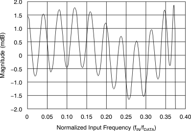 Figure 40. FIR Passband Magnitude Response (FDATA = 500 Hz)
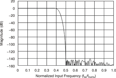 Figure 41. FIR Transition Band Magnitude Response
Although not shown in Figure 41, the passband response repeats at multiples of the modulator frequency (NƒMOD – ƒ0 and NƒMOD + ƒ0, where N = 1, 2, and so forth, and ƒ0 = passband). These image frequencies, if present in the signal and not externally filtered, fold back (or alias) into the passband and cause errors. A low-pass signal filter reduces the effect of aliasing. Often, the RC low-pass filter provided by the PGA output resistors and the external capacitor connected to CAPP and CAPN provides sufficient signal attenuation.
8.3.13.3 Group Delay and Step Response
The FIR block is implemented as a multi-stage FIR structure with selectable linear or minimum phase response. The passband, transition band, and stop band responses of the filters are nearly identical but differ in the respective phase responses.
8.3.13.3.1 Linear Phase Response
Linear phase filters exhibit constant delay time versus input frequency (that is, constant group delay). Linear phase filters have the property that the time delay from any instant of the input signal to the same instant of the output data is constant and is independent of the signal nature. This filter behavior results in essentially zero phase error when analyzing multi-tone signals. However, the group delay and settling time of the linear phase filter are somewhat larger than the minimum phase filter, as shown in Figure 42.
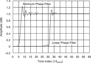 Figure 42. FIR Step Response
8.3.13.3.2 Minimum Phase Response
The minimum phase filter provides a short delay from the arrival of an input signal to the output, but the relationship (phase) is not constant versus frequency, as shown in Figure 43. The filter phase is selected by the PHS bit, as Table 7 shows.
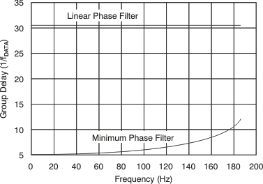 Figure 43. FIR Group Delay (FDATA = 500 Hz)
Table 7. Fir Phase Selection
| PHS BIT | FILTER PHASE |
|---|---|
| 0 | Linear |
| 1 | Minimum |
8.3.13.4 HPF Stage
The last stage of the ADS1282-HT filter block is a first-order HPF implemented as an IIR structure. This filter stage blocks DC signals and rolls off low-frequency components below the cut-off frequency. The transfer function for the filter is shown in Equation 16 of the 器件支持.
The high-pass corner frequency is programmed by registers HPF[1:0], in hexadecimal. Equation 10 is used to set the high-pass corner frequency. Table 8 lists example values for the high-pass filter.

where
- HPF = High-pass filter register value (converted to hexadecimal)
- ωN = 2πƒHP/ƒDATA (normalized frequency, radians)
- ƒHP = High-pass corner frequency (Hz)
- ƒDATA = Data rate (Hz)
Table 8. High-Pass Filter Value Examples
| ƒHP (Hz) | DATA RATE (SPS) | HPF[1:0] |
|---|---|---|
| 0.5 | 250 | 0337h |
| 1 | 500 | 0337h |
| 1 | 1000 | 019Ah |
The HPF causes a small gain error, in which case the magnitude of the error depends on the ratio of ƒHP/ƒDATA. For many common values of (ƒHP/ƒDATA), the gain error is negligible. Figure 44 shows the gain error of the HPF. The gain error factor is illustrated in Equation 15 (see 器件支持).
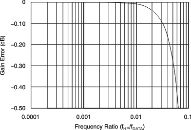 Figure 44. HPF Gain Error
Figure 45 shows the first-order amplitude and phase response of the HPF. In the case of applying step inputs or synchronizing, the settling time of the filter should be taken into account.
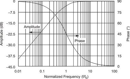 Figure 45. HPF Amplitude and Phase Response
8.3.14 Master Clock Input (CLK)
The ADS1282-HT requires a clock input for operation. The clock is applied to the CLK pin. The data conversion rate scales directly with the CLK frequency. Power consumption versus CLK frequency is relatively constant (see the Typical Characteristics).
As with any high-speed data converter, a high-quality, low-jitter clock is essential for optimum performance. Crystal clock oscillators are the recommended clock source. Make sure to avoid excess ringing on the clock input; keep the clock trace as short as possible and use a 50-Ω series resistor close to the source.
8.3.15 Synchronization (SYNC Pin and Sync Command)
The ADS1282-HT can be synchronized to an external event, as well as synchronized to other ADS1282-HT devices if the sync event is applied simultaneously.
The ADS1282-HT has two sources for synchronization: the SYNC input pin and the SYNC command. The ADS1282-HT also has two synchronizing modes: Pulse-sync and Continuous-sync. In Pulse-sync mode, the ADS1282-HT synchronizes to a single sync event. In Continuous-sync mode, either a single SYNC event is used to synchronize conversions or a continuous clock is applied to the pin with a period equal to integer multiples of the data rate. When the periods of the sync input and the DRDY output do not match, the ADS1282-HT re-synchronizes and conversions are restarted.
8.3.16 Pulse-Sync Mode
In pulse-sync mode, the ADS1282-HT stops and restarts the conversion process when a sync event occurs (by pin or command). When the sync event occurs, the device resets the internal memory; DRDY goes high (pulse SYNC mode) otherwise in Continuous SYNC mode, DRDY continues to toggle, and after the digital filter has settled, new conversion data are available, as shown in Figure 46 and Pulse-Sync Timing Requirements.
Resynchronization occurs on the next rising CLK edge after the rising edge of the SYNC pin or after the eighth rising SCLK edge for opcode SYNC commands. To be effective, the SYNC opcode should be broadcast to all devices simultaneously.
8.3.17 Continuous-Sync Mode
In Continuous-sync mode, either a single sync pulse or a continuous clock may be applied. When a single sync pulse is applied (rising edge), the device behaves similar to the Pulse-sync mode. However, in this mode, DRDY continues to toggle unaffected but the DOUT output is held low until data are ready, 63 DRDY periods later. When the conversion data are non-zero, new conversion data are ready (as shown in Figure 46).
When a continuous clock is applied to the SYNC pin, the period must be an integral multiple of the output data rate or the device re-synchronizes. Synchronization results in the restarting of the digital filter and an interruption of 63 readings (refer to Pulse-Sync Timing Requirements).
When the sync input is first applied, the device re-synchronizes (under the condition tSYNC ≠ N / ƒDATA). DRDY continues to output but DOUT is held low until the new data are ready. Then, if SYNC is applied again and the period matches an integral multiple of the output data rate, the device freely runs without re-synchronization. The phase of the applied clock and output data rate (DRDY) are not matched because of the initial delay of DRDY after SYNC is first applied. Figure 47 shows the timing for Continuous-Sync mode.
A SYNC clock input should be applied after the Continuous-Sync mode is set. The first rising edge of SYNC then causes a synchronization.
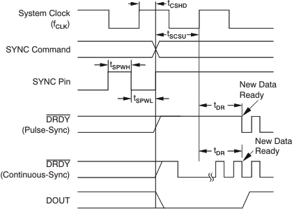 Figure 46. Pulse-Sync Timing, Continuous-Sync Timing With Single Sync
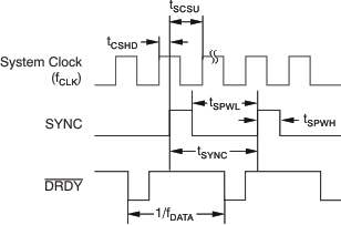 Figure 47. Continuous-Sync Timing With Sync Clock
8.3.18 Reset (RESET Pin and Reset Command)
The ADS1282-HT may be reset in two ways: toggle the RESET pin low or send a Reset command. When using the RESET pin, take it low and hold for at least 2 / ƒCLK to force a reset. The ADS1282-HT is held in reset until the pin is released. By command, RESET takes effect on the next rising edge of ƒCLK after the eighth rising edge of SCLK of the command. To ensure the Reset command can function, the SPI interface may require resetting itself; see Serial Interface.
In reset, registers are set to default and the conversions are synchronized on the next rising edge of CLK. New conversion data are available, as shown in Figure 48 and Reset Timing Requirements.
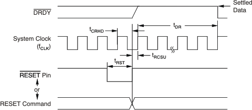 Figure 48. Reset Timing
8.3.19 Power-Down (PWDN Pin and Standby Command)
There are two ways to power-down the ADS1282-HT: take the PWDN pin low or send a Standby command. When the PWDN pin is pulled low, the internal circuitry is disabled to minimize power and the contents of the register settings are reset.
In power-down, the device outputs remain active and the device inputs must not float. When the Standby command is sent, the SPI port and the configuration registers are kept active. Figure 49 and Pulse-Sync Timing Requirements show the timing.
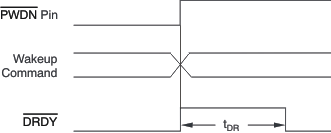 Figure 49. PWDN Pin and Wake-Up Command Timing
(Pulse-Sync Timing Requirements Shows tDR)
8.3.20 Power-On Sequence
The ADS1282-HT has three power supplies: AVDD, AVSS, and DVDD. Figure 50 shows the power-on sequence of the ADS1282-HT. The power supplies can be sequenced in any order. The supplies [the difference of (AVDD – AVSS) and DVDD] generate an internal reset whose outputs are summed to generate a global internal reset. After the supplies have crossed the minimum thresholds, 216 ƒCLK cycles are counted before releasing the internal reset. After the internal reset is released, new conversion data are available, as shown in Figure 50 and Pulse-Sync Timing Requirements.
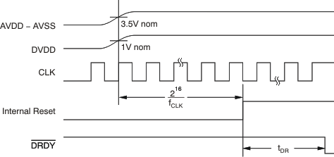 Figure 50. Power-On Sequence
8.3.21 Serial Interface
A serial interface is used to read the conversion data and access the configuration registers. The interface consists of three basic signals: SCLK, DIN, and DOUT. An additional output, DRDY, transitions low in Read Data Continuous mode when data are ready for retrieval. Figure 51 shows the connection when multiple converters are used.
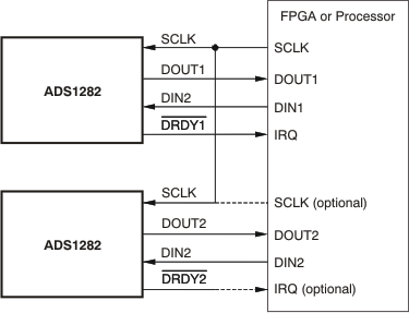 Figure 51. Interface for Multiple Devices
8.3.21.1 Serial Clock (SCLK)
The serial clock (SCLK) is an input that is used to clock data into (DIN) and out of (DOUT) the ADS1282-HT. This input is a Schmitt-trigger input that has a high degree of noise immunity. However, TI recommends keeping SCLK as clean as possible to prevent possible glitches from inadvertently shifting the data.
Data are shifted into DIN on the rising edge of SCLK and data are shifted out of DOUT on the falling edge of SCLK. If SCLK is held low for 64 DRDY cycles, data transfer or commands in progress terminate and the SPI interface resets. The next SCLK pulse starts a new communication cycle. This time-out feature can be used to recover the interface when a transmission is interrupted or SCLK inadvertently glitches. SCLK should remain low when not active.
8.3.21.2 Data Input (DIN)
The data input pin (DIN) is used to input register data and commands to the ADS1282-HT. Keep DIN low when reading conversion data in the Read Data Continuous mode (except when issuing a STOP Read Data Continuous command). Data on DIN are shifted into the converter on the rising edge of SCLK. In Pin mode, DIN is not used.
8.3.21.3 Data Output (DOUT)
The data output pin (DOUT) is used to output data from the ADS1282-HT. Data are shifted out on DOUT on the falling edge of SCLK.
8.3.21.4 Data Ready (DRDY)
DRDY is an output; when it transitions low, this transition indicates new conversion data are ready, as shown in Figure 52. When reading data by the continuous mode, the data must be read within four CLK periods before DRDY goes low again or the data are overwritten with new conversion data. When reading data by the command mode, the read operation can overlap the occurrence of the next DRDY without data corruption.
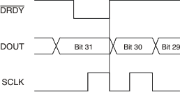 Figure 52. DRDY With Data Retrieval
DRDY resets high on the first falling edge of SCLK. Figure 52 and Figure 53 show the function of DRDY with and without data readback, respectively.
If data are not retrieved (no SCLK provided), DRDY pulses high for four ƒCLK periods during the update time, as shown in Figure 53.
 Figure 53. DRDY With No Data Retrieval
8.3.22 Data Format
The ADS1282-HT provides 32 bits of conversion data in binary twos complement format, as shown in Table 9. The LSB of the data is a redundant sign bit: '0' for positive numbers and '1' for negative numbers. However, when the output is clipped to +FS, the LSB = 1; when the output is clipped to –FS, the LSB = 0. If desired, the data readback may be stopped at 24 bits. In sinc filter mode, the output data are scaled by 1/2.
Table 9. Ideal Output Code Versus Input Signal
| INPUT SIGNAL VIN
(AINP – AINN) |
32-BIT IDEAL OUTPUT CODE(1) | |||
|---|---|---|---|---|
| FIR FILTER | SINC FILTER(2) | |||
 |
7FFFFFFFh | (3) | ||
 |
7FFFFFFEh | 3FFFFFFFh | ||
 |
00000002h | 00000001h | ||
| 0 | 00000000h | 00000000h | ||
 |
FFFFFFFFh | FFFFFFFFh | ||
 |
80000001h | C0000000h | ||
 |
80000000h | (3) | ||
- Excludes effects of noise, linearity, offset, and gain errors.
- Due to the reduction in oversampling ratio (OSR) related to the sinc filter high data rates, full 32-bit available resolution is reduced.
- In sinc filter mode, the output does not clip at half-scale code when the full-scale range is exceeded.
8.3.23 Reading Data
The ADS1282-HT has two ways to read conversion data: Read Data Continuous and Read Data By Command.
8.3.23.1 Read Data Continuous
In the Read Data Continuous mode, the conversion data are shifted out directly from the device without the need for sending a read command. This mode is the default mode at power-on. This mode is also enabled by the RDATAC command. When DRDY goes low, indicating that new data are available, the MSB of data appears on DOUT, as shown in Figure 54. The data are normally read on the rising edge of SCLK, at the occurrence of the first falling edge of SCLK, DRDY returns high. After 32 bits of data have been shifted out, further SCLK transitions cause DOUT to go low. If desired, the read operation may be stopped at 24 bits. The data shift operation must be completed within four CLK periods before DRDY falls again or the data may be corrupted.
When a Stop Read Data Continuous command is issued, the DRDY output is blocked but the ADS1282-HT continues conversions. In stop continuous mode, the data can only be read by command.
8.3.23.2 Read Data by Command
The Read Data Continuous mode is stopped by the SDATAC command. In this mode, conversion data are read by command. In the Read Data By Command mode, a read data command must be sent to the device for each data conversion (as shown in Figure 55). When the read data command is received (on the eighth SCLK rising edge), data are available to read only when DRDY goes low (tDR). When DRDY goes low, conversion data appear on DOUT. The data may be read on the rising edge of SCLK.
 Figure 54. Read Data Continuous
 Figure 55. Read Data By Command, Rdata (TDDPD Timing Is Given In Read Data Timing Requirements)
8.3.24 One-Shot Operation
The ADS1282-HT can perform very power-efficient, one-shot conversions using the STANDBY command while under software control. Figure 73 shows this sequence. First, issue the STANDBY command to set the Standby mode.
When ready to make a measurement, issue the WAKEUP command. Monitor DRDY; when it goes low, the fully settled conversion data are ready and may be read directly in Read Data Continuous mode. Afterwards, issue another STANDBY command. When ready for the next measurement, repeat the cycle starting with another WAKEUP command.
8.4 Device Functional Modes
8.4.1 Modulator Output Mode
The modulator digital stream output is accessible directly, bypassing and disabling the internal digital filter. The modulator output mode is activated by setting the CONFIG0 register bits FILTR[1:0] = 00. Pins M0 and M1 then become the modulator data outputs and the MCLK becomes the modulator clock output. When not in the modulator mode, these pins are inputs and must be tied.
The modulator output is composed of three signals: one output for the modulator clock (MCLK) and two outputs for the modulator data (M0 and M1). The modulator clock output rate is ƒMOD (ƒCLK / 4). The SYNC input resets the MCLK phase, as shown in Figure 56. The SYNC input is latched on the rising edge of CLK. The MCLK resets and the next rising edge of MCLK occurs five CLK periods later.
The modulator output data are two bits wide, which must be merged together before being filtered. Use the time domain equation of Equation 5 to merge the data outputs.
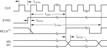
NOINDENT:
MCLK = ƒCLK / 4.8.5 Programming
8.5.1 Commands
The commands listed in Table 10 control the operation of the ADS1282-HT. Most commands are stand-alone (that is, 1 byte in length); the register reads and writes require a second command byte in addition to the actual data bytes.
A delay of 24 ƒCLK cycles between commands and between bytes within a command is required, starting from the last SCLK rising edge of one command to the first SCLK rising edge of the following command. This delay is shown in Figure 57.
In Read Data Continuous mode, the ADS1282-HT places conversion data on the DOUT pin as SCLK is applied. As a consequence of the potential conflict of conversion data on DOUT and data placed on DOUT resulting from a register or Read Data By Command operation, it is necessary to send a STOP Read Data Continuous command before Register or Data Read By Command. The STOP Read Data Continuous command disables the direct output of conversion data on the DOUT pin.

Table 10. Command Descriptions
| COMMAND | TYPE | DESCRIPTION | 1st COMMAND BYTE(1)(2) | 2nd COMMAND BYTE(3) |
|---|---|---|---|---|
| WAKEUP | Control | Wake-up from Standby mode | 0000 000X (00h or 01h) | |
| STANDBY | Control | Enter Standby mode | 0000 001X (0 h or 03h) | |
| SYNC | Control | Synchronize the A/D conversion | 0000 010X (04h or 5h) | |
| RESET | Control | Reset registers to default values | 0000 011X (06h or 07h) | |
| RDATAC | Control | Read data continuous | 0001 0000 (10h) | |
| SDATAC | Control | Stop read data continuous | 0001 0001 (11h) | |
| RDATA | Data | Read data by command(4) | 0001 0010 (12h) | |
| RREG | Register | Read nnnnn register(s) at address rrrrr(4) | 00r rrrr (20h + 000r rrrr) | 000n nnnn (00h + n nnnn) |
| WREG | Register | Write nnnnn register(s) at address rrrrr | 010r rrrr (40h + 000r rrrr) | 000n nnnn (00h + n nnnn) |
| OFSCAL | Calibration | Offset calibration | 0110 0000 (60h) | |
| GANCAL | Calibration | Gain calibration | 0110 0001 (61h) |
8.5.1.1 WAKEUP: Wake-Up from Standby Mode
This command is used to exit the standby mode. Upon sending the command, the time for the first data to be ready is illustrated in Figure 49 and Table 9. Sending this command during normal operation has no effect; for example, reading data by the Read Data Continuous method with DIN held low.
8.5.1.2 STANDBY: Standby Mode
This command places the ADS1282-HT into Standby mode. In Standby, the device enters a reduced power state where a low quiescent current remains to keep the register settings and SPI interface active. For complete device shutdown, take the PWDN pin low (register settings are not saved). To exit Standby mode, issue the WAKEUP command. The operation of Standby mode is shown in Figure 58.
 Figure 58. Standby Command Sequence
8.5.1.3 SYNC: Synchronize the A/D Conversion
This command synchronizes the A/D conversion. Upon receipt of the command, the reading in progress is cancelled and the conversion process is re-started. In order to synchronize multiple ADS1282-HTs, the command must be sent simultaneously to all devices. The SYNC pin must be high for this command.
8.5.1.4 RESET: Reset the Device
The RESET command resets the registers to default values, enables the Read Data Continuous mode, and restarts the conversion process; the RESET command is functionally the same as the RESET pin. See Figure 48 for the RESET command timing.
8.5.1.5 RDATAC: Read Data Continuous
This command enables the Read Data Continuous mode (default mode). In this mode, conversion data can be read from the device directly without the need to supply a data read command. Each time DRDY falls low, new data are available to read. See Read Data Continuous for more details.
8.5.1.6 SDATAC: Stop Read Data Continuous
This command stops the Read Data Continuous mode. Exiting the Read Data Continuous mode is required before sending Register and Data read commands. This command suppresses the DRDY output, but the ADS1282-HT continues conversions.
8.5.1.7 RDATA: Read Data By Command
This command reads the conversion data. See Read Data by Command for more details.
8.5.1.8 RREG: Read Register Data
This command is used to read single or multiple register data. The command consists of a two-byte op-code argument followed by the output of register data. The first byte of the op-code includes the starting address, and the second byte specifies the number of registers to read – 1.
First command byte: 001r rrrr, where rrrrr is the starting address of the first register.
Second command byte: 000n nnnn, where nnnnn is the number of registers – 1 to read.
Starting with the 16th falling edge of SCLK, the register data appear on DOUT.
The RREG command is illustrated in Figure 59. The a delay of 24 ƒCLK cycles is required between each byte transaction.
8.5.1.9 WREG: Write to Register
This command writes single or multiple register data. The command consists of a two-byte op-code argument followed by the input of register data. The first byte of the op-code contains the starting address and the second byte specifies the number of registers to write – 1.
First command byte: 001r rrrr, where rrrrr is the starting address of the first register.
Second command byte: 000n nnnn, where nnnnn is the number of registers – 1 to write.
Data byte(s): one or more register data bytes, depending on the number of registers specified.
Figure 60 illustrates the WREG command.
A delay of 24 ƒCLK cycles is required between each byte transaction.
8.5.1.10 OFSCAL: Offset Calibration
This command performs an offset calibration. The inputs to the converter (or the inputs to the external pre-amplifier) should be zeroed and allowed to stabilize before sending this command. The offset calibration register updates after this operation. See Calibration Commands for more details.
8.5.1.11 GANCAL: Gain Calibration
This command performs a gain calibration. The inputs to the converter should have a stable DC input, preferably close to (but not exceeding) positive full-scale. The gain calibration register updates after this operation. See Calibration Commands for more details.
 Figure 59. Read Register Data ( Shows tDLY)
8.5.2 Calibration Commands
Calibration commands may be sent to the ADS1282-HT to calibrate the conversion data. The values of the offset and gain calibration registers are internally written to perform calibration. The appropriate input signals must be applied to the ADS1282-HT inputs before sending the commands. Use slower data rates to achieve more consistent calibration results; this effect is a byproduct of the lower noise that these data rates provide. Also, if calibrating at power-on, be sure the reference voltage is fully settled.
Figure 61 shows the calibration command sequence. After the analog input voltage (and reference) have stabilized, send the Stop Data Continuous command followed by the SYNC and Read Data Continuous commands. 64 data periods later, DRDY goes low. After DRDY goes low, send the Stop Data Continuous, then the Calibrate command followed by the Read Data Continuous command. After 16 data periods, calibration is complete and conversion data may be read at this time. The SYNC input must remain high during the calibration sequence.
The calibration commands apply to specific PGA settings. If the PGA is changed, recalibration is necessary. Calibration is bypassed in the sinc filter mode.
8.5.2.1 OFSCAL Command
The OFSCAL command performs an offset calibration. Before sending the offset calibration command, a zero input signal must be applied to the ADS1282-HT and the inputs allowed to stabilize. When the command is sent, the ADS1282-HT averages 16 readings and then writes this value to the OFC register. The contents of the OFC register may be subsequently read or written. During offset calibration, the full-scale correction is bypassed.
8.5.2.2 GANCAL Command
The GANCAL command performs a gain calibration. Before sending the GANCAL command, a DC input signal must be applied that is in the range of, but not exceeding, positive or negative full-scale. After the signal has stabilized, the command can be sent. The ADS1282-HT averages 16 readings, then computes the value that compensates for the gain error. The gain correction value is then written to the FSC register. The contents of the GANCAL register may be subsequently read or written. While the gain calibration command corrects for gain errors greater than 1 (gain correction <1), to avoid input overload, the analog inputs cannot exceed full-scale range. The gain calibration should be performed after the offset calibration.
 Figure 61. Offset/Gain Calibration Timing
8.5.3 User Calibration
System calibration of the ADS1282-HT can be performed without using the calibration commands. This procedure requires the calibration values to be externally calculated and then written to the calibration registers. The steps for this procedure are:
- Set the OFSCAL[2:0] register = 0h and GANCAL[2:0] = 400000h. These values set the offset and gain registers to 0 and 1, respectively.
- Apply a zero differential input to the input of the system. Wait for the system to settle and then average n output readings. Higher numbers of averaged readings result in more consistent calibration. Write the averaged value to the OFC register.
- Apply a differential positive or negative DC signal, or an AC signal, less than the full-scale input to the system. Wait for the system to settle and then average the n output readings.
The value written to the FSC registers is calculated by Equation 12.
DC signal calibration is shown in Equation 12. The expected output code is based on 31-bit output data.

For AC signal calibration, use an RMS value of collected data (as shown in Equation 13).

8.5.4 Configuration Guide
After RESET or power-on, the registers can be configured using the following procedure:
- Reset the serial interface. Before using the serial interface, it may be necessary to recover the serial interface (undefined I/O power-up sequencing may cause false SCLK detection). To reset the SPI interface, toggle the RESET pin or, when in Read Data Continuous mode, hold SCLK low for 64 DRDY periods.
- Configure the registers. The registers are configured by either writing to them individually or as a group. Software may be configured in either mode. The SDATAC command must be sent before register read/write operations to cancel the Read Data Continuous mode.
- Verify register data. The register may be read back for verification of device communications.
- Set the data mode. After register configuration, the device may be configured for Read Data Continuous mode, either by the Read Data Continuous command or configured in Read Data By Register mode using SDATAC command.
- Synchronize readings. Whenever SYNC is high, the ADS1282-HT freely runs the data conversions. To stop and re-sync the conversions, take SYNC low and then high.
- Read data. If the Read Data Continuous mode is active, the data are read directly after DRDY falls by applying SCLK pulses. If the Read Data Continuous mode is inactive, the data can only be read by Read Data By Command. The Read Data opcode command must be sent in this mode to read each conversion result (DRDY only asserts after each read data command is sent).
8.6 Register Maps
8.6.1 ADS1282-HT Register Map Information
Collectively, the registers contain all the information needed to configure the part, such as data rate, filter selection, calibration, and so forth. The registers are accessed by the RREG and WREG commands. The registers can be accessed individually or as a block of registers by sending or receiving consecutive bytes. After a register write operation the ADC resets, resulting in an interruption of 63 readings.
Table 11. ADS1282-HT Register Map
| ADDRESS | REGISTER | RESET VALUE | BIT 7 | BIT 6 | BIT 5 | BIT 4 | BIT 3 | BIT 2 | BIT 1 | BIT 0 |
|---|---|---|---|---|---|---|---|---|---|---|
| 00h | ID | X0h | ID3 | ID2 | ID1 | ID0 | 0 | 0 | 0 | 0 |
| 01h | CONFIG0 | 52h | SYNC | MODE | DR2 | DR1 | DR0 | PHS | FILTR1 | FILTR0 |
| 02h | CONFIG1 | 08h | 0 | MUX2 | MUX1 | MUX0 | CHOP | PGA2 | PGA1 | PGA0 |
| 03h | HPF0 | 32h | HPF07 | HPF06 | HPF05 | HPF04 | HPF03 | HPF02 | HPF01 | HPF00 |
| 04h | HPF1 | 03h | HPF15 | HPF14 | HPF13 | HPF12 | HPF11 | HPF10 | HPF09 | HPF08 |
| 05h | OFC0 | 00h | OFC07 | OFC06 | OFC05 | OFC04 | OFC03 | OFC02 | OFC01 | OFC00 |
| 06h | OFC1 | 00h | OFC15 | OFC14 | OFC13 | OFC12 | OFC11 | OFC10 | OFC09 | OFC08 |
| 07h | OFC2 | 00h | OFC23 | OFC22 | OFC21 | OFC20 | OFC19 | OFC18 | OFC17 | OFC16 |
| 08h | FSC0 | 00h | FSC07 | FSC06 | FSC05 | FSC04 | FSC03 | FSC02 | FSC01 | FSC00 |
| 09h | FSC1 | 00h | FSC15 | FSC14 | FSC13 | FSC12 | FSC11 | FSC10 | FSC09 | FSC08 |
| 0Ah | FSC2 | 40h | FSC23 | FSC22 | FSC21 | FSC20 | FSC19 | FSC18 | FSC17 | FSC16 |
8.6.2 ID Register
| 7 | 6 | 5 | 4 | 3 | 2 | 1 | 0 |
| ID3 | ID2 | ID1 | ID0 | Reserved | |||
| 0 | 0 | 0 | 0 | ||||
| Reset value = X0h |
Table 12. ID Register Field Descriptions
| Bit | Field | Type | Reset | Description |
|---|---|---|---|---|
| 7:4 | ID[3:0] | Factory-programmed identification bits (read-only) | ||
| 3:0 | Reserved | Always write '0' |
8.6.3 Configuration Registers
8.6.3.1 Configuration Register 0
| 7 | 6 | 5 | 4 | 3 | 2 | 1 | 0 |
| SYNC | MODE | DR2 | DR1 | DR0 | PHASE | FILTR1 | FILTR0 |
| Reset value = 52h |
Table 13. Configuration Register 0 Field Descriptions
| Bit | Field | Type | Reset | Description |
|---|---|---|---|---|
| 7 | SYNC | Synchronization mode 0: Pulse SYNC mode (default) 1: Continuous SYNC mode |
||
| 6 | MODE | 1: High-resolution mode (default) | ||
| 5:3 | DR[2:0] | Data Rate Select(1)
000: 250SPS 001: 500SPS 010: 1000SPS (default) 011: 2000SPS 100: 4000SPS |
||
| 2 | PHASE | FIR Phase Response 0: Linear phase (default) 1: Minimum phase |
||
| 1:0 | FILTR[1:0] | Digital Filter Select Digital filter configuration 00: On-chip filter bypassed, modulator output mode 01: Sinc filter block only 10: Sinc + LPF filter blocks (default) 11: Sinc + LPF + HPF filter blocks |
8.6.3.2 Configuration Register 1
| 7 | 6 | 5 | 4 | 3 | 2 | 1 | 0 |
| RSVD | MUX2 | MUX1 | MUX0 | CHOP | PGA2 | PGA1 | PGA0 |
| 0 |
| Reset value = 08h |
Table 14. Configuration Register 1 Field Descriptions
| Bit | Field | Type | Reset | Description |
|---|---|---|---|---|
| 7 | Reserved | Always write '0' | ||
| 6:4 | MUX[2:0] | MUX Select 000: AINP1 and AINN1 (default) 001: AINP2 and AINN2 010: Internal short via 400Ω 011:AINP1 and AINN1 connected to AINP2 and AINN2 100: External short to AINN2 |
||
| 3 | CHOP | PGA Chopping Enable 0: PGA chopping disabled 1: PGA chopping enabled (default) |
||
| 2:0 | PGA[2:0] | PGA Gain Select 000: G = 1 (default) 001: G = 2 010: G = 4 011: G = 8 100: G = 16 101: G = 32 110: G = 64 |
8.6.4 HPF1 and HPF0
These two bytes (high-byte and low-byte, respectively) set the corner frequency of the high-pass filter.
8.6.4.1 High-Pass Filter Corner Frequency, Low Byte
| 7 | 6 | 5 | 4 | 3 | 2 | 1 | 0 |
| HP07 | HP06 | HP05 | HP04 | HP03 | HP02 | HP01 | HP00 |
| Reset value = 32h |
8.6.4.2 High-Pass Filter Corner Frequency, High Byte
| 7 | 6 | 5 | 4 | 3 | 2 | 1 | 0 |
| HP15 | HP14 | HP13 | HP12 | HP11 | HP10 | HP09 | HP08 |
| Reset value = 03h |
8.6.5 OFC2, OFC1, OFC0
These three bytes set the offset calibration value.
8.6.5.1 Offset Calibration, Low Byte
| 7 | 6 | 5 | 4 | 3 | 2 | 1 | 0 |
| OC07 | OC06 | OC05 | OC04 | OC03 | OC02 | OC01 | OC00 |
| Reset value = 00h |
8.6.5.2 Offset Calibration, Mid Byte
| 7 | 6 | 5 | 4 | 3 | 2 | 1 | 0 |
| OC15 | OC14 | OC13 | OC12 | OC11 | OC10 | OC09 | OC08 |
| Reset value = 00h |
8.6.5.3 Offset Calibration, High Byte
| 7 | 6 | 5 | 4 | 3 | 2 | 1 | 0 |
| OC23 | OC22 | OC21 | OC20 | OC19 | OC18 | OC17 | OC16 |
| Reset value = 00h |
8.6.6 FSC2, FSC1, FSC0
These three bytes set the full-scale calibration value.
8.6.6.1 Full-Scale Calibration, Low Byte
| 7 | 6 | 5 | 4 | 3 | 2 | 1 | 0 |
| FSC07 | FSC06 | FSC05 | FSC04 | FSC03 | FSC02 | FSC01 | FSC00 |
| Reset value = 00h |
8.6.6.2 Full-Scale Calibration, Mid Byte
| 7 | 6 | 5 | 4 | 3 | 2 | 1 | 0 |
| FSC15 | FSC14 | FSC13 | FSC12 | FSC11 | FSC10 | FSC09 | FSC08 |
| Reset value = 00h |
8.6.6.3 Full-Scale Calibration, High Byte
| 7 | 6 | 5 | 4 | 3 | 2 | 1 | 0 |
| FSC23 | FSC22 | FSC21 | FSC20 | FSC19 | FSC18 | FSC17 | FSC16 |
| Reset value = 40h |
8.6.7 Offset and Full-Scale Calibration Registers
The conversion data can be scaled for offset and gain before yielding the final output code. As shown in Figure 74, the output of the digital filter is first subtracted by the offset register (OFC) and then multiplied by the full-scale register (FSC). Equation 14 shows the scaling:

The values of the offset and full-scale registers are set by writing to them directly, or they are set automatically by calibration commands.
The offset and full-scale calibrations apply to specific PGA settings. When the PGA changes, the contents of these registers may have to be recalculated. Calibration is bypassed in the sinc filter mode.

NOINDENT:
See Figure 49 and for time to new data. Figure 74. Calibration Block Diagram
8.6.7.1 OFC[2:0] Registers
The offset calibration is a 24-bit word, composed of three 8-bit registers, as shown in Table 17. The offset register is left-justified to align with the 32-bits of conversion data. The offset is in twos complement format with a maximum positive value of 7FFFFFh and a maximum negative value of 800000h. This value is subtracted from the conversion data. A register value of 00000h has no offset correction (default value). While the offset calibration register value can correct offsets ranging from –FS to +FS (as shown in Table 15), to avoid input overload, the analog inputs cannot exceed the full-scale range.
Table 15. Offset Calibration Values
| OFC REGISTER | FINAL OUTPUT CODE(1) |
|---|---|
| 7FFFFFh | 80000000h |
| 000001h | FFFFFF00h |
| 000000h | 00000000h |
| FFFFFFh | 00000100h |
| 800000h | 7FFFFF00h |
8.6.7.2 FSC[2:0] Registers
The full-scale calibration is a 24-bit word, composed of three 8-bit registers, as shown in Table 18. The full-scale calibration value is 24-bit, straight offset binary, normalized to 1 at code 400000h. Table 16 summarizes the scaling of the full-scale register. A register value of 400000h (default value) has no gain correction (gain = 1). While the gain calibration register value corrects gain errors greater than 1 (gain correction <1), the full-scale range of the analog inputs cannot be exceeded to avoid input overload.
Table 16. Full-Scale Calibration Register Values
| FSC REGISTER | GAIN CORRECTION |
|---|---|
| 800000h | 2 |
| 400000h | 1 |
| 200000h | 0.5 |
| 000000h | 0 |
Table 17. Offset Calibration Word
| REGISTER | BYTE | BIT ORDER | |||||||
|---|---|---|---|---|---|---|---|---|---|
| OFC0 | LSB | 7 | 6 | 5 | 4 | 3 | 2 | 1 | 0 (LSB) |
| OFC1 | MID | 15 | 14 | 13 | 12 | 11 | 10 | 9 | 8 |
| OFC2 | MSB | 23 (MSB) | 22 | 21 | 20 | 19 | 18 | 17 | 16 |
Table 18. Full-Scale Calibration Word
| REGISTER | BYTE | BIT ORDER | |||||||
|---|---|---|---|---|---|---|---|---|---|
| FSC0 | LSB | 7 | 6 | 5 | 4 | 3 | 2 | 1 | 0 (LSB) |
| FSC1 | MID | 15 | 14 | 13 | 12 | 11 | 10 | 9 | 8 |
| FSC2 | MSB | 23 (MSB) | 22 | 21 | 20 | 19 | 18 | 17 | 16 |
