ZHCSES2H December 2009 – February 2016 ADS1282-HT
PRODUCTION DATA.
- 1 特性
- 2 应用
- 3 说明
- 4 修订历史记录
- 5 说明 (续)
- 6 Pin Configuration and Functions
-
7 Specifications
- 7.1 Absolute Maximum Ratings
- 7.2 Recommended Operating Conditions
- 7.3 Thermal Information
- 7.4 Electrical Characteristics
- 7.5 Electrical Characteristics (PW Package)
- 7.6 Timing Requirements
- 7.7 Pulse-Sync Timing Requirements
- 7.8 Reset Timing Requirements
- 7.9 Switching Characteristics
- 7.10 Modulator Switching Characteristics
- 7.11 Typical Characteristics
-
8 Detailed Description
- 8.1 Overview
- 8.2 Functional Block Diagram
- 8.3
Feature Description
- 8.3.1 Noise Performance
- 8.3.2 Input-Referred Noise
- 8.3.3 Idle Tones
- 8.3.4 Operating Mode
- 8.3.5 Analog Inputs and Multiplexer
- 8.3.6 PGA (Programmable Gain Amplifier)
- 8.3.7 ADC
- 8.3.8 Modulator
- 8.3.9 Modulator Over-Range
- 8.3.10 Modulator Input Impedance
- 8.3.11 Modulator Over-Range Detection (MFLAG)
- 8.3.12 Voltage Reference Inputs (VREFP, VREFN)
- 8.3.13 Digital Filter
- 8.3.14 Master Clock Input (CLK)
- 8.3.15 Synchronization (SYNC Pin and Sync Command)
- 8.3.16 Pulse-Sync Mode
- 8.3.17 Continuous-Sync Mode
- 8.3.18 Reset (RESET Pin and Reset Command)
- 8.3.19 Power-Down (PWDN Pin and Standby Command)
- 8.3.20 Power-On Sequence
- 8.3.21 Serial Interface
- 8.3.22 Data Format
- 8.3.23 Reading Data
- 8.3.24 One-Shot Operation
- 8.4 Device Functional Modes
- 8.5
Programming
- 8.5.1
Commands
- 8.5.1.1 WAKEUP: Wake-Up from Standby Mode
- 8.5.1.2 STANDBY: Standby Mode
- 8.5.1.3 SYNC: Synchronize the A/D Conversion
- 8.5.1.4 RESET: Reset the Device
- 8.5.1.5 RDATAC: Read Data Continuous
- 8.5.1.6 SDATAC: Stop Read Data Continuous
- 8.5.1.7 RDATA: Read Data By Command
- 8.5.1.8 RREG: Read Register Data
- 8.5.1.9 WREG: Write to Register
- 8.5.1.10 OFSCAL: Offset Calibration
- 8.5.1.11 GANCAL: Gain Calibration
- 8.5.2 Calibration Commands
- 8.5.3 User Calibration
- 8.5.4 Configuration Guide
- 8.5.1
Commands
- 8.6 Register Maps
- 9 Application and Implementation
- 10Power Supply Recommendations
- 11器件和文档支持
- 12机械、封装和可订购信息
封装选项
机械数据 (封装 | 引脚)
散热焊盘机械数据 (封装 | 引脚)
- PW|28
订购信息
9 Application and Implementation
NOTE
Information in the following applications sections is not part of the TI component specification, and TI does not warrant its accuracy or completeness. TI’s customers are responsible for determining suitability of components for their purposes. Customers should validate and test their design implementation to confirm system functionality.
9.1 Application Information
The ADS1282-HT is a very-high-resolution ADC. Optimal performance requires giving special attention to the support circuitry and PCB design. Locate noisy digital components, such as microcontrollers, oscillators, and so forth, in an area of the PCB away from the converter or front-end components. Locating the digital components close to the power-entry point keeps the digital current path short and separate from sensitive analog components.
9.2 Typical Application
9.2.1 Geophone Interface Typical Application
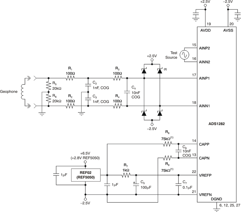
Figure 75 shows a typical geophone front-end application. The application shows the ADS1282-HT operation with dual ±2.5-V analog supplies. The ADS1282-HT can also operate with a single 5-V analog supply.

NOINDENT:
Optional 20-mV offset. Match to 0.1% to maintain CMR.9.2.1.1 Detailed Design Procedure
The geophone input signal is filtered both differentially, by components C4 and R1 to R4 and filtered independently by components C2, C3 and R1, R2. The differential filter removes high-frequency normal mode components from the input signal. The independent filters remove high-frequency components that are common to both input signals leads (common-mode filter). The recommended input filters may not be required for all applications depending on the system requirements.
Resistors R5 and R6 bias the signals inputs to midsupply (ground), and also provide the bias current return path for the ADS1282-HT inputs. For single-supply operation, set the bias to a low impedance 2.5 V (AVDD/2). Resistors R5 and R6 can also influence common-mode attenuation. To maintain good CMR performance, resistors R5 and R6 may require matching.
Diode clamps protect the ADS1282-HT inputs from voltage transients and overloads.
The REF02 5-V reference provides the reference to the ADS1282-HT. The reference output is filtered by the optional R7 and C5 filter network. The filter requires several seconds to settle after power-on. Capacitor C7 provides high-frequency bypassing of the reference inputs and should be placed close to the ADS1282-HT pins. R7 (1-kΩ) results in a systematic gain error (–1.2%).
Alternatively, the REF5050 (5-V) or REF5045 (4.5-V) reference can be used. The REF5045 reference has the advantage of operating from the 5-V power supply. The REF5050 requires 5.2-V minimum power supply.
Optional components R8, and R9 provides a 20mV offset to the ADS1282-HT. The internal 300-Ω resistors form a voltage divider with the external resistors to provide the offset. The offset moves the low level idle tones out of the passband. The offset is independent of the PGA setting. To maintain good CMR performance, R10 and R11 should be matched to 0.1%, and the traces routed back directly to the reference.
Capacitor C6 (10-nF) filters the PGA output glitches caused by sampling of the modulator. The capacitor also forms a low-pass filter on the input signal with a cut-off frequency ≉ 25 kHz.
9.2.2 Digital Connection to a Field Programmable Gate Array (FPGA) Device Typical Application
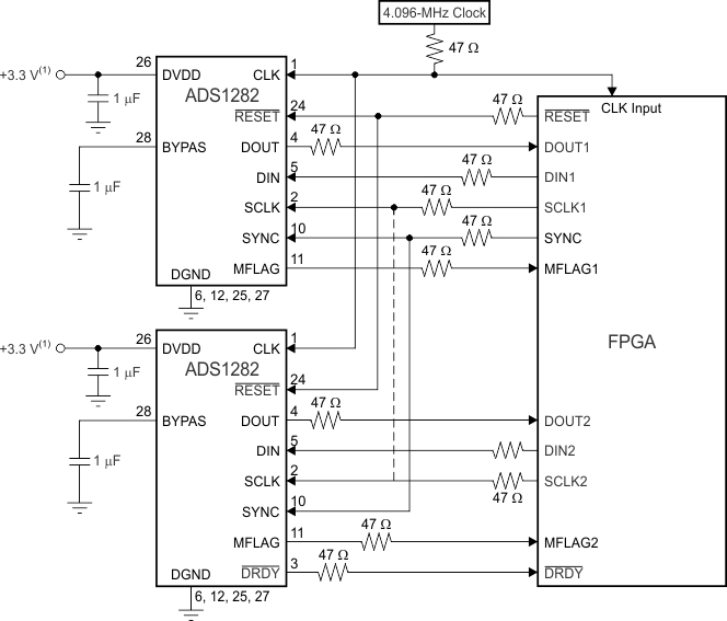
Figure 76 shows the digital connection to a field programmable gate array (FPGA) device. In this example, two ADS1282-HT devices are shown connected. The DRDY output from each ADS1282-HT device can be used; however, when the devices are synchronized, the DRDY output from only one device is sufficient. A shared SCLK line between the devices is optional.

NOINDENT:
NOTE: Dashed line is optional.NOINDENT:
For DVDD < 2.25 V, see the Power Supply Recommendations.9.2.2.1 Detailed Design Procedure
The modulator over-range flag (MFLAG) from each device ties to the FPGA. For synchronization, one SYNC control line connects all ADS1282-HT devices. The RESET line also connects to all ADS1282-HT devices.
For best performance, the FPGA and the ADS1282-HTs should operate from the same clock. Avoid ringing on the digital inputs. 47-Ω resistors in series with the digital traces can help to reduce ringing by controlling impedances. Place the resistors at the source (driver) end of the trace. Unused digital inputs should not float; use pullups or pulldowns to DVDD or GND. This includes the modulator data pins, M0, M1, and MCLK.