SNAS298G August 2005 – January 2015 ADC128S102
PRODUCTION DATA.
6 Specifications
6.1 Absolute Maximum Ratings
See (1)(2).| MIN | MAX | UNIT | ||
|---|---|---|---|---|
| Analog Supply Voltage VA | −0.3 | 6.5 | V | |
| Digital Supply Voltage VD | −0.3 | VA + 0.3, max 6.5 | V | |
| Voltage on Any Pin to GND | −0.3 | VA +0.3 | V | |
| Input Current at Any Pin (3) | –10 | 10 | mA | |
| Package Input Current(3) | –20 | 20 | mA | |
| Power Dissipation at TA = 25°C | See (4) | |||
| Junction Temperature | 150 | °C | ||
| Storage temperature, Tstg | −65 | 150 | °C | |
| For soldering specifications: see product folder at www.ti.com and SNOA549 | ||||
(1) Stresses beyond those listed under Absolute Maximum Ratings may cause permanent damage to the device. These are stress ratings only, which do not imply functional operation of the device at these or any other conditions beyond those indicated under Recommended Operating Conditions. Exposure to absolute-maximum-rated conditions for extended periods may affect device reliability.
(2) If Military/Aerospace specified devices are required, please contact the TI Sales Office/ Distributors for availability and specifications.
(3) When the input voltage at any pin exceeds the power supplies (that is, VIN < AGND or VIN > VA or VD), the current at that pin should be limited to 10 mA. The 20 mA maximum package input current rating limits the number of pins that can safely exceed the power supplies with an input current of 10 mA to two.
(4) The absolute maximum junction temperature (TJmax) for this device is 150°C. The maximum allowable power dissipation is dictated by TJmax, the junction-to-ambient thermal resistance (θJA), and the ambient temperature (TA), and can be calculated using the formula PDMAX = (TJmax − TA)/θJA. In the 16-pin TSSOP, θJA is 96°C/W, so PDMAX = 1,200 mW at 25°C and 625 mW at the maximum operating ambient temperature of 105°C. Note that the power consumption of this device under normal operation is a maximum of 12 mW. The values for maximum power dissipation listed above will be reached only when the ADC128S102 is operated in a severe fault condition (e.g. when input or output pins are driven beyond the power supply voltages, or the power supply polarity is reversed). Obviously, such conditions should always be avoided.
6.2 ESD Ratings
| VALUE | UNIT | |||
|---|---|---|---|---|
| V(ESD) | Electrostatic discharge | Human body model (HBM), per ANSI/ESDA/JEDEC JS-001(1) | ±2500 | V |
| Machine model (MM) | ±250 | |||
(1) JEDEC document JEP155 states that 500-V HBM allows safe manufacturing with a standard ESD control process.
6.3 Recommended Operating Conditions
over operating free-air temperature range (unless otherwise noted)(1)| MIN | MAX | UNIT | |
|---|---|---|---|
| Operating Temperature, TA | –40 | 105 | °C |
| VA Supply Voltage | 2.7 | 5.25 | V |
| VD Supply Voltage | 2.7 | VA | V |
| Digital Input Voltage | 0 | VA | V |
| Analog Input Voltage | 0 | VA | V |
| Clock Frequency | 8 | 16 | MHz |
(1) All voltages are measured with respect to GND = 0V, unless otherwise specified.
6.4 Thermal Information
| THERMAL METRIC(1) | ADC128S102 | UNIT | |
|---|---|---|---|
| PW | |||
| 16 PINS | |||
| RθJA | Junction-to-ambient thermal resistance | 110 | °C/W |
| RθJC(top) | Junction-to-case (top) thermal resistance | 42 | |
| RθJB | Junction-to-board thermal resistance | 56 | |
| ψJT | Junction-to-top characterization parameter | 5 | |
| ψJB | Junction-to-board characterization parameter | 55 | |
(1) For more information about traditional and new thermal metrics, see the IC Package Thermal Metrics application report, SPRA953.
6.5 Electrical Characteristics
The following specifications apply for TA = 25°C, AGND = DGND = 0 V, fSCLK = 8 MHz to 16 MHz, fSAMPLE = 500 ksps to 1 MSPS, CL = 50pF, unless otherwise noted. MIN and MAX limits apply for TA = TMIN to TMAX.(2)| PARAMETER | TEST CONDITIONS | MIN | TYP | MAX(1) | UNIT | |
|---|---|---|---|---|---|---|
| STATIC CONVERTER CHARACTERISTICS | ||||||
| Resolution with No Missing Codes | 12 | Bits | ||||
| INL | Integral Non-Linearity (End Point Method) | VA = VD = +3.0V | –1 | ±0.4 | 1 | LSB |
| VA = VD = +5.0V | –1.2 | ±0.5 | 1.2 | LSB | ||
| DNL | Differential Non-Linearity | VA = VD = +3.0V | +0.4 | 0.9 | LSB | |
| −0.7 | −0.2 | LSB | ||||
| VA = VD = +5.0V | +0.7 | 1.5 | LSB | |||
| −0.9 | −0.4 | LSB | ||||
| VOFF | Offset Error | VA = VD = +3.0V | –2.3 | +0.8 | 2.3 | LSB |
| VA = VD = +5.0V | –2.3 | +1.1 | 2.3 | LSB | ||
| OEM | Offset Error Match | VA = VD = +3.0V | –1.5 | ±0.1 | 1.5 | LSB |
| VA = VD = +5.0V | –1.5 | ±0.3 | 1.5 | LSB | ||
| FSE | Full Scale Error | VA = VD = +3.0V | –2.0 | +0.8 | 2.0 | LSB |
| VA = VD = +5.0V | –2.0 | +0.3 | 2.0 | LSB | ||
| FSEM | Full Scale Error Match | VA = VD = +3.0V | –1.5 | ±0.1 | 1.5 | LSB |
| VA = VD = +5.0V | –1.5 | ±0.3 | 1.5 | LSB | ||
| DYNAMIC CONVERTER CHARACTERISTICS | ||||||
| FPBW | Full Power Bandwidth (−3dB) | VA = VD = +3.0V | 8 | MHz | ||
| VA = VD = +5.0V | 11 | MHz | ||||
| SINAD | Signal-to-Noise Plus Distortion Ratio | VA = VD = +3.0V, fIN = 40.2 kHz, −0.02 dBFS |
70 | 73 | dB | |
| VA = VD = +5.0V, fIN = 40.2 kHz, −0.02 dBFS |
70 | 73 | dB | |||
| SNR | Signal-to-Noise Ratio | VA = VD = +3.0V, fIN = 40.2 kHz, −0.02 dBFS |
70.8 | 73 | dB | |
| VA = VD = +5.0V, fIN = 40.2 kHz, −0.02 dBFS |
70.8 | 73 | dB | |||
| THD | Total Harmonic Distortion | VA = VD = +3.0V, fIN = 40.2 kHz, −0.02 dBFS |
−88 | −74 | dB | |
| VA = VD = +5.0V, fIN = 40.2 kHz, −0.02 dBFS |
−90 | −74 | dB | |||
| SFDR | Spurious-Free Dynamic Range | VA = VD = +3.0V, fIN = 40.2 kHz, −0.02 dBFS |
75 | 91 | dB | |
| VA = VD = +5.0V, fIN = 40.2 kHz, −0.02 dBFS |
75 | 92 | dB | |||
| ENOB | Effective Number of Bits | VA = VD = +3.0V, fIN = 40.2 kHz |
11.3 | 11.8 | Bits | |
| VA = VD = +5.0V, fIN = 40.2 kHz, −0.02 dBFS |
11.3 | 11.8 | Bits | |||
| ISO | Channel-to-Channel Isolation | VA = VD = +3.0V, fIN = 20 kHz |
82 | dB | ||
| VA = VD = +5.0V, fIN = 20 kHz, −0.02 dBFS |
84 | dB | ||||
| IMD | Intermodulation Distortion, Second Order Terms | VA = VD = +3.0V, fa = 19.5 kHz, fb = 20.5 kHz |
−89 | dB | ||
| VA = VD = +5.0V, fa = 19.5 kHz, fb = 20.5 kHz |
−91 | dB | ||||
| Intermodulation Distortion, Third Order Terms | VA = VD = +3.0V, fa = 19.5 kHz, fb = 20.5 kHz |
−88 | dB | |||
| VA = VD = +5.0V, fa = 19.5 kHz, fb = 20.5 kHz |
−88 | dB | ||||
| ANALOG INPUT CHARACTERISTICS | ||||||
| VIN | Input Range | 0 to VA | V | |||
| IDCL | DC Leakage Current | –1 | 1 | µA | ||
| CINA | Input Capacitance | Track Mode | 33 | pF | ||
| Hold Mode | 3 | pF | ||||
| DIGITAL INPUT CHARACTERISTICS | ||||||
| VIH | Input High Voltage | VA = VD = +2.7V to +3.6V | 2.1 | V | ||
| VA = VD = +4.75V to +5.25V | 2.4 | V | ||||
| VIL | Input Low Voltage | VA = VD = +2.7V to +5.25V | 0.8 | V | ||
| IIN | Input Current | VIN = 0V or VD | –1 | ±0.01 | 1 | µA |
| CIND | Digital Input Capacitance | 2 | 4 | pF | ||
| DIGITAL OUTPUT CHARACTERISTICS | ||||||
| VOH | Output High Voltage | ISOURCE = 200 µA, VA = VD = +2.7V to +5.25V |
VD − 0.5 | V | ||
| VOL | Output Low Voltage | ISINK = 200 µA to 1.0 mA, VA = VD = +2.7V to +5.25V |
0.4 | V | ||
| IOZH, IOZL | Hi-Impedance Output Leakage Current | VA = VD = +2.7V to +5.25V | –1 | 1 | µA | |
| COUT | Hi-Impedance Output Capacitance (2) | 2 | 4 | pF | ||
| Output Coding | Straight (Natural) Binary | |||||
| POWER SUPPLY CHARACTERISTICS (CL = 10 pF) | ||||||
| VA, VD | Analog and Digital Supply Voltages | VA ≥ VD | 2.7 | 5.25 | V | |
| IA + ID | Total Supply Current Normal Mode ( CS low) |
VA = VD = +2.7V to +3.6V, fSAMPLE = 1 MSPS, fIN = 40 kHz |
0.76 | 1.5 | mA | |
| VA = VD = +4.75V to +5.25V, fSAMPLE = 1 MSPS, fIN = 40 kHz |
2.13 | 3.1 | mA | |||
| Total Supply Current Shutdown Mode (CS high) |
VA = VD = +2.7V to +3.6V, fSCLK = 0 ksps |
20 | nA | |||
| VA = VD = +4.75V to +5.25V, fSCLK = 0 ksps |
50 | nA | ||||
| PC | Power Consumption Normal Mode ( CS low) |
VA = VD = +3.0V fSAMPLE = 1 MSPS, fIN = 40 kHz |
2.3 | 4.5 | mW | |
| VA = VD = +5.0V fSAMPLE = 1 MSPS, fIN = 40 kHz |
10.7 | 15.5 | mW | |||
| Power Consumption Shutdown Mode (CS high) |
VA = VD = +3.0V fSCLK = 0 ksps |
0.06 | µW | |||
| VA = VD = +5.0V fSCLK = 0 ksps |
0.25 | µW | ||||
| AC ELECTRICAL CHARACTERISTICS | ||||||
| fSCLKMIN | Minimum Clock Frequency | VA = VD = +2.7V to +5.25V | 8 | 0.8 | MHz | |
| fSCLK | Maximum Clock Frequency | VA = VD = +2.7V to +5.25V | 16 | MHz | ||
| fS | Sample Rate Continuous Mode |
VA = VD = +2.7V to +5.25V | 500 | 50 | ksps | |
| 1 | MSPS | |||||
| tCONVERT | Conversion (Hold) Time | VA = VD = +2.7V to +5.25V | 13 | SCLK cycles | ||
| DC | SCLK Duty Cycle | VA = VD = +2.7V to +5.25V | 40% | 30 | ||
| 70 | 60% | |||||
| tACQ | Acquisition (Track) Time | VA = VD = +2.7V to +5.25V | 3 | SCLK cycles | ||
| Throughput Time | Acquisition Time + Conversion Time VA = VD = +2.7V to +5.25V |
16 | SCLK cycles | |||
| tAD | Aperture Delay | VA = VD = +2.7V to +5.25V | 4 | ns | ||
(1) Tested limits are specified to TI's AOQL (Average Outgoing Quality Level).
(2) Data sheet min/max specification limits are ensured by design, test, or statistical analysis.
6.6 Timing Specifications
The following specifications apply for TA = 25°C, VA = VD = +2.7V to +5.25V, AGND = DGND = 0V, fSCLK = 8 MHz to 16 MHz, fSAMPLE = 500 ksps to 1 MSPS, and CL = 50pF. MIN and MAX apply for TA = TMIN to TMAX.| PARAMETER | TEST CONDITIONS | MIN | TYP | MAX(1) | UNIT | |
|---|---|---|---|---|---|---|
| tCSH | CS Hold Time after SCLK Rising Edge | 10 | 0 | ns | ||
| tCSS | CS Setup Time prior to SCLK Rising Edge | 10 | 4.5 | ns | ||
| tEN | CS Falling Edge to DOUT enabled | 5 | 30 | ns | ||
| tDACC | DOUT Access Time after SCLK Falling Edge | 17 | 27 | ns | ||
| tDHLD | DOUT Hold Time after SCLK Falling Edge | 4 | ns | |||
| tDS | DIN Setup Time prior to SCLK Rising Edge | 10 | 3 | ns | ||
| tDH | DIN Hold Time after SCLK Rising Edge | 10 | 3 | ns | ||
| tCH | SCLK High Time | 0.4 x tSCLK | ns | |||
| tCL | SCLK Low Time | 0.4 x tSCLK | ns | |||
| tDIS | CS Rising Edge to DOUT High-Impedance | DOUT falling | 2.4 | 20 | ns | |
| DOUT rising | 0.9 | 20 | ns | |||
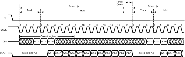 Figure 1. ADC128S102 Operational Timing Diagram
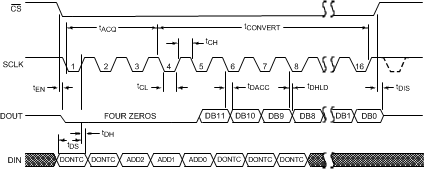 Figure 2. ADC128S102 Serial Timing Diagram
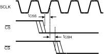 Figure 3. SCLK and CS Timing Parameters
6.7 Typical Characteristics
TA = +25°C, fSAMPLE = 1 MSPS, fSCLK = 16 MHz, fIN = 40.2 kHz unless otherwise stated.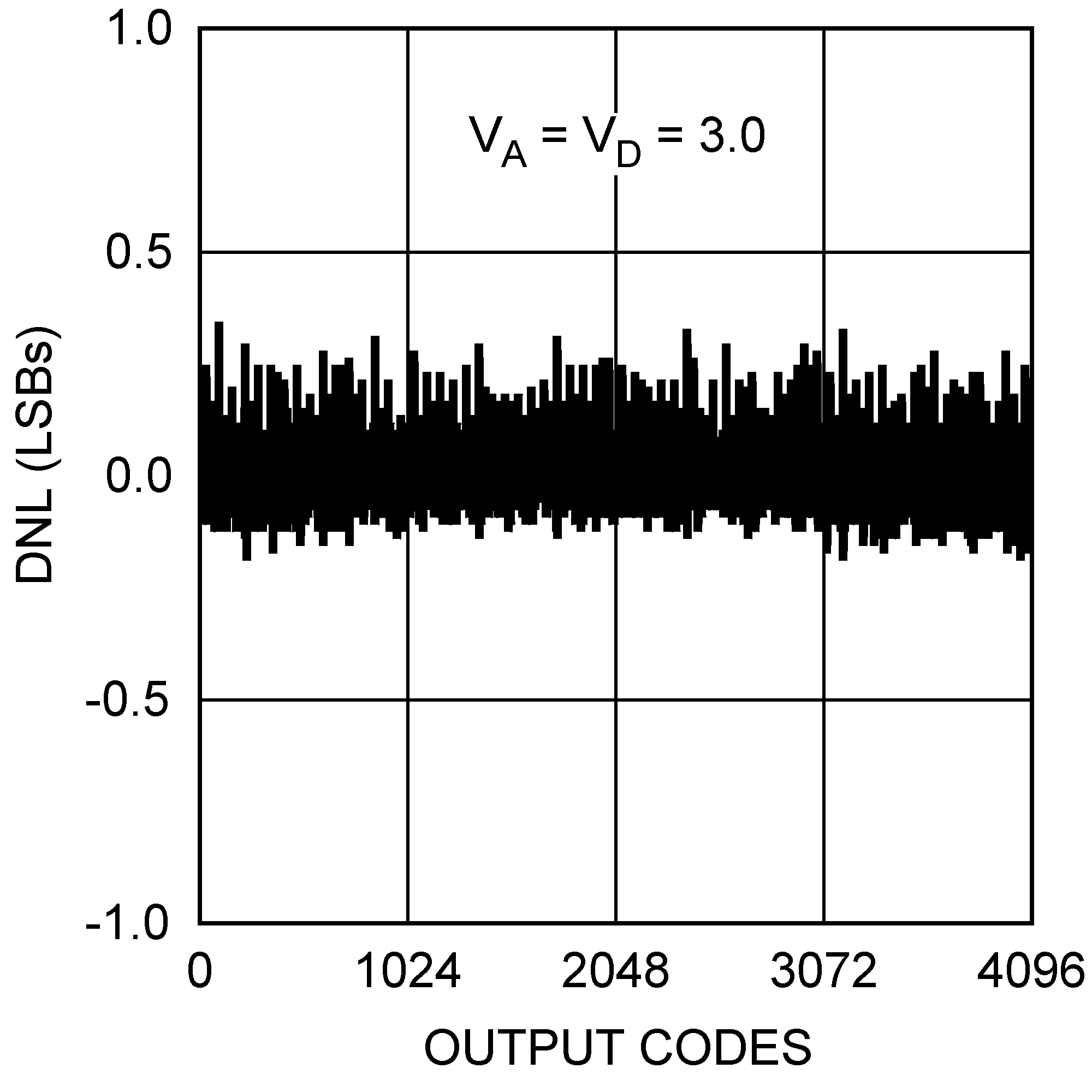 Figure 4. DNL
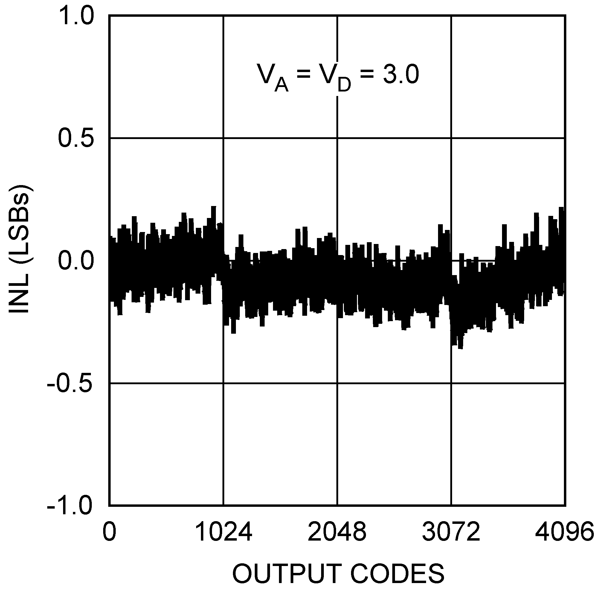 Figure 6. INL
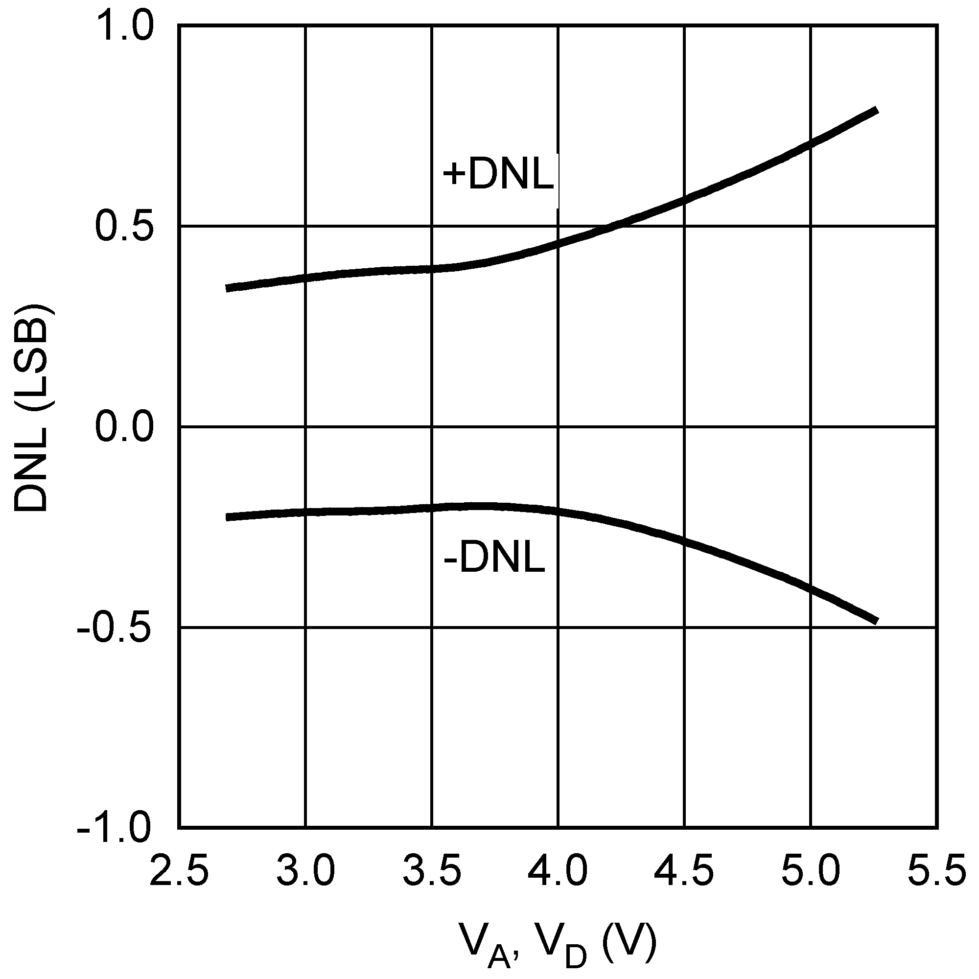 Figure 8. DNL vs. Supply
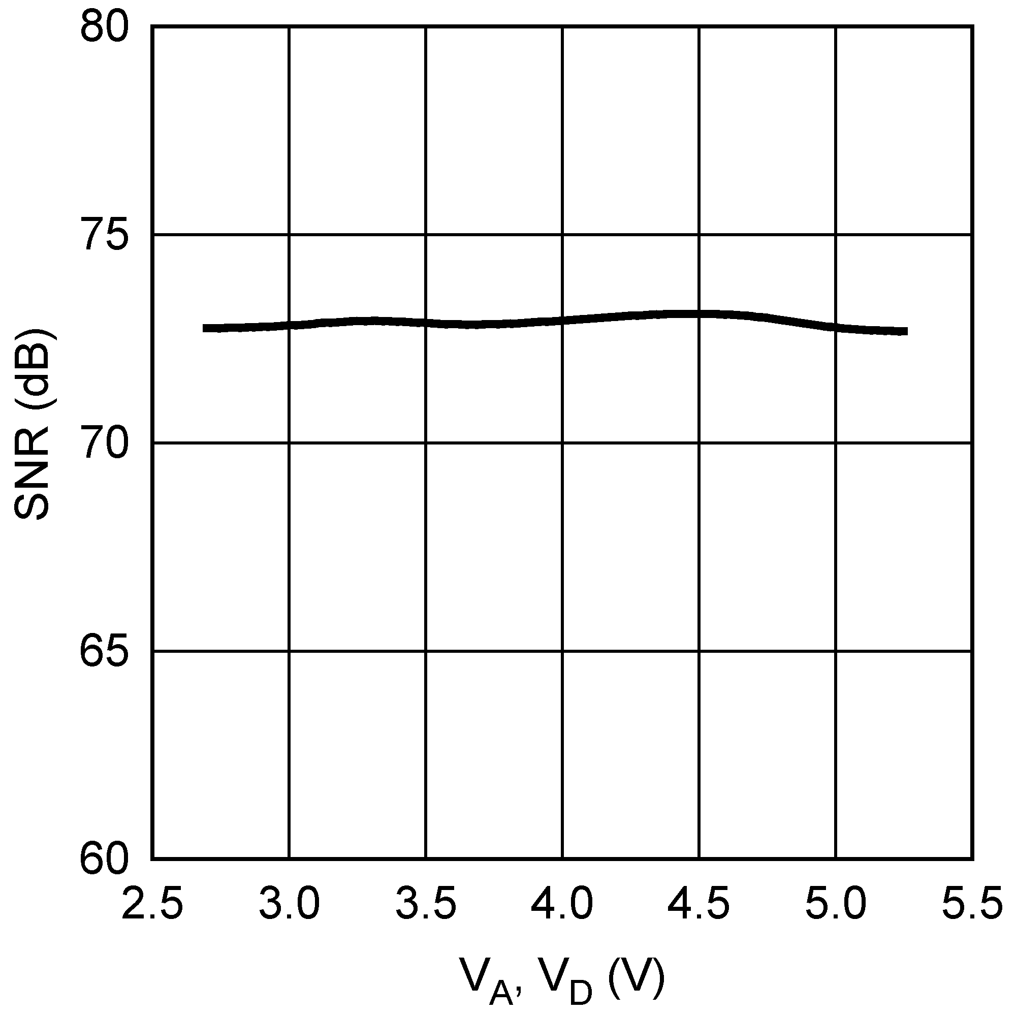 Figure 10. SNR vs. Supply
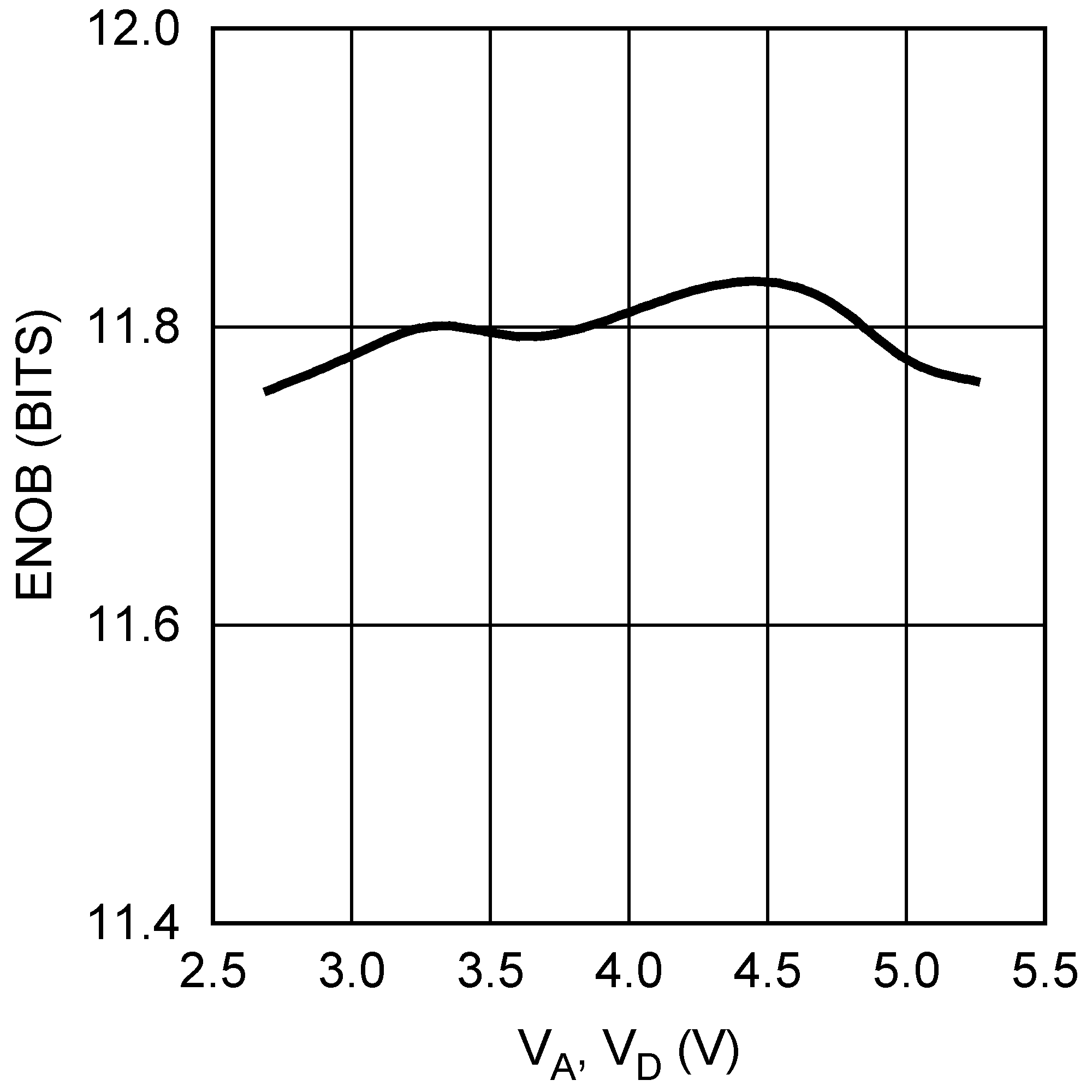 Figure 12. ENOB vs. Supply
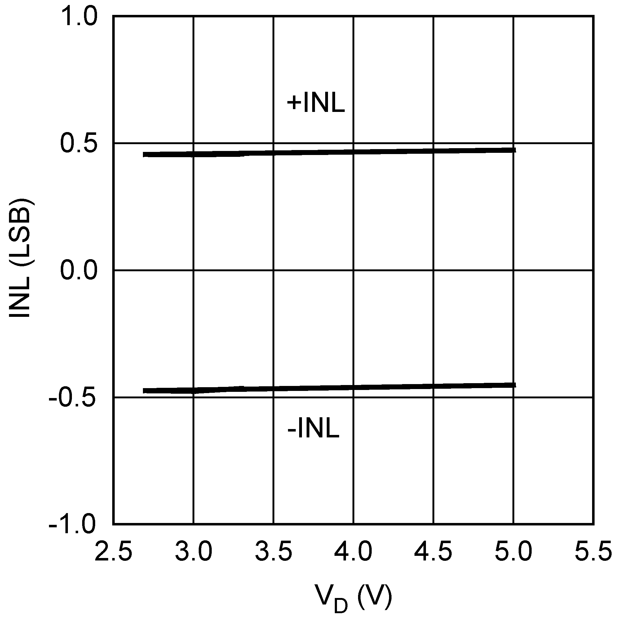 Figure 14. INL vs. VD with VA = 5.0 V
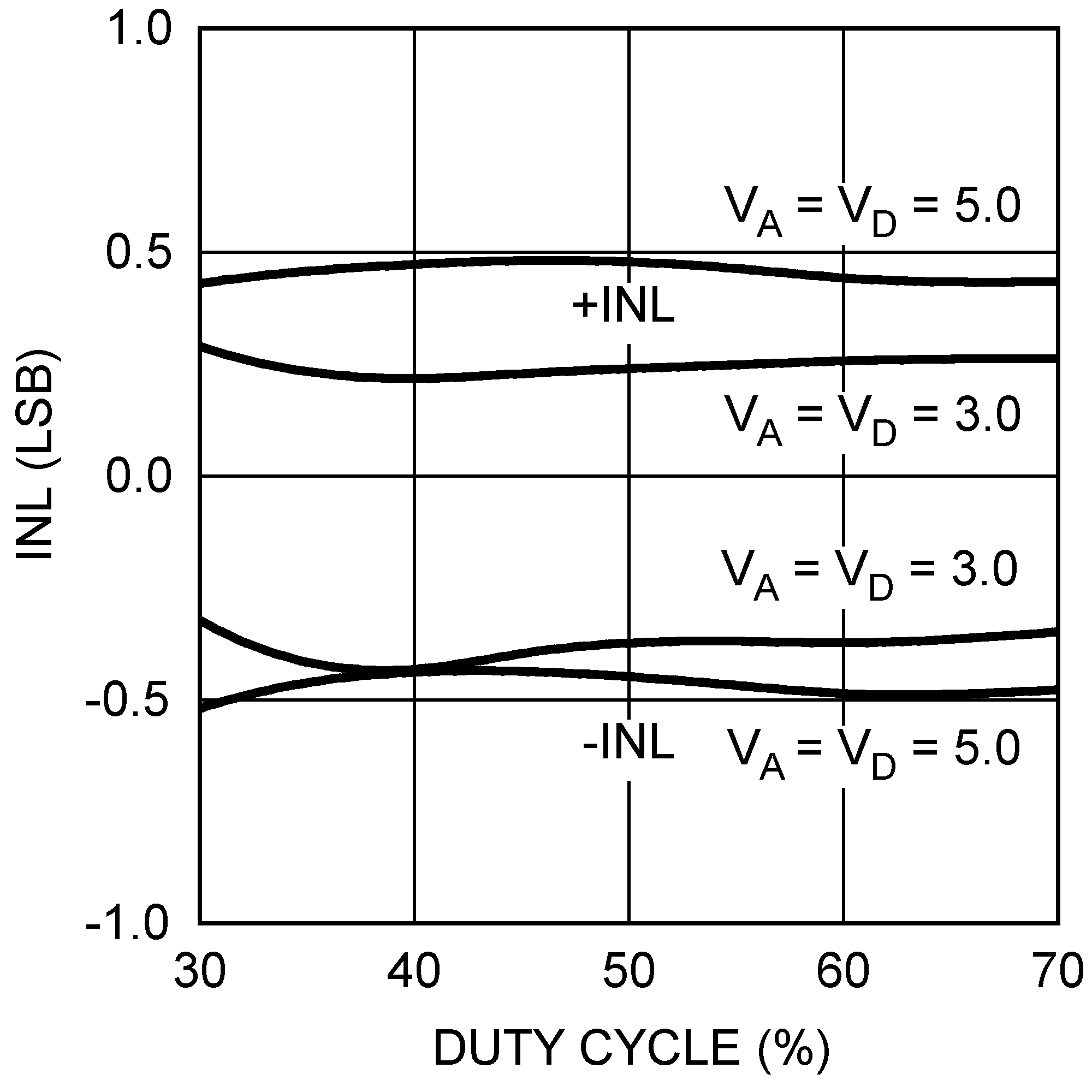 Figure 16. INL vs. SCLK Duty Cycle
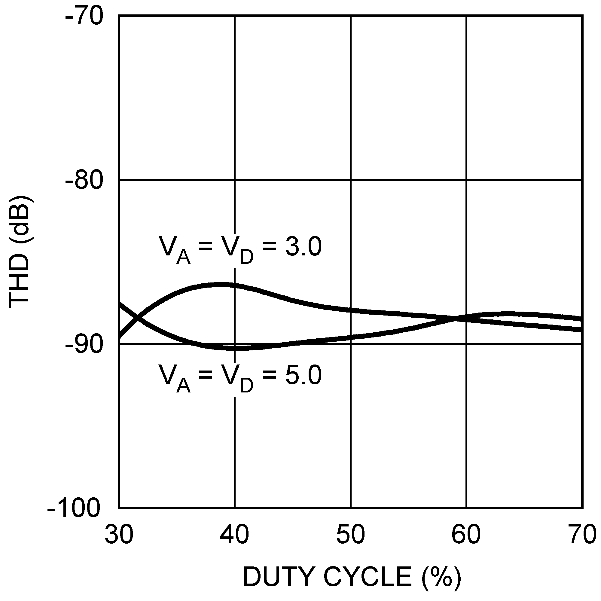 Figure 18. THD vs. SCLK Duty Cycle
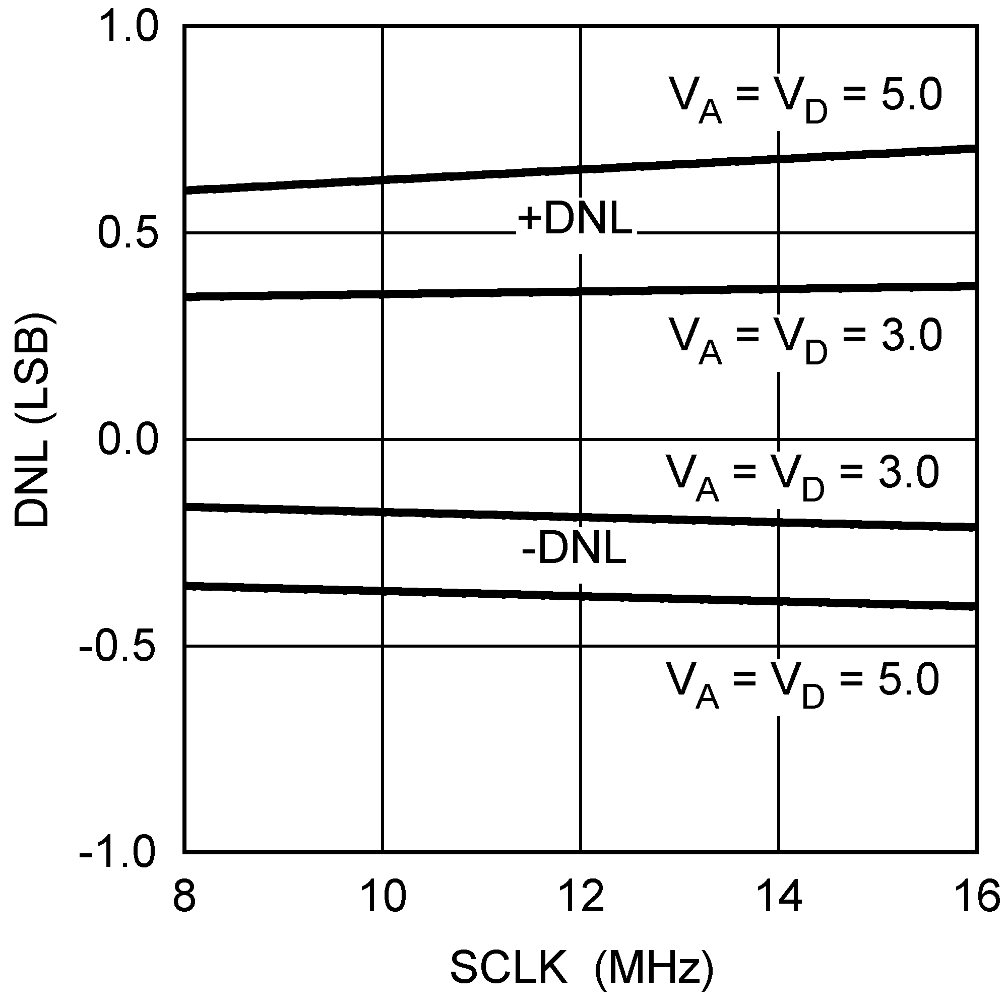 Figure 20. DNL vs. SCLK
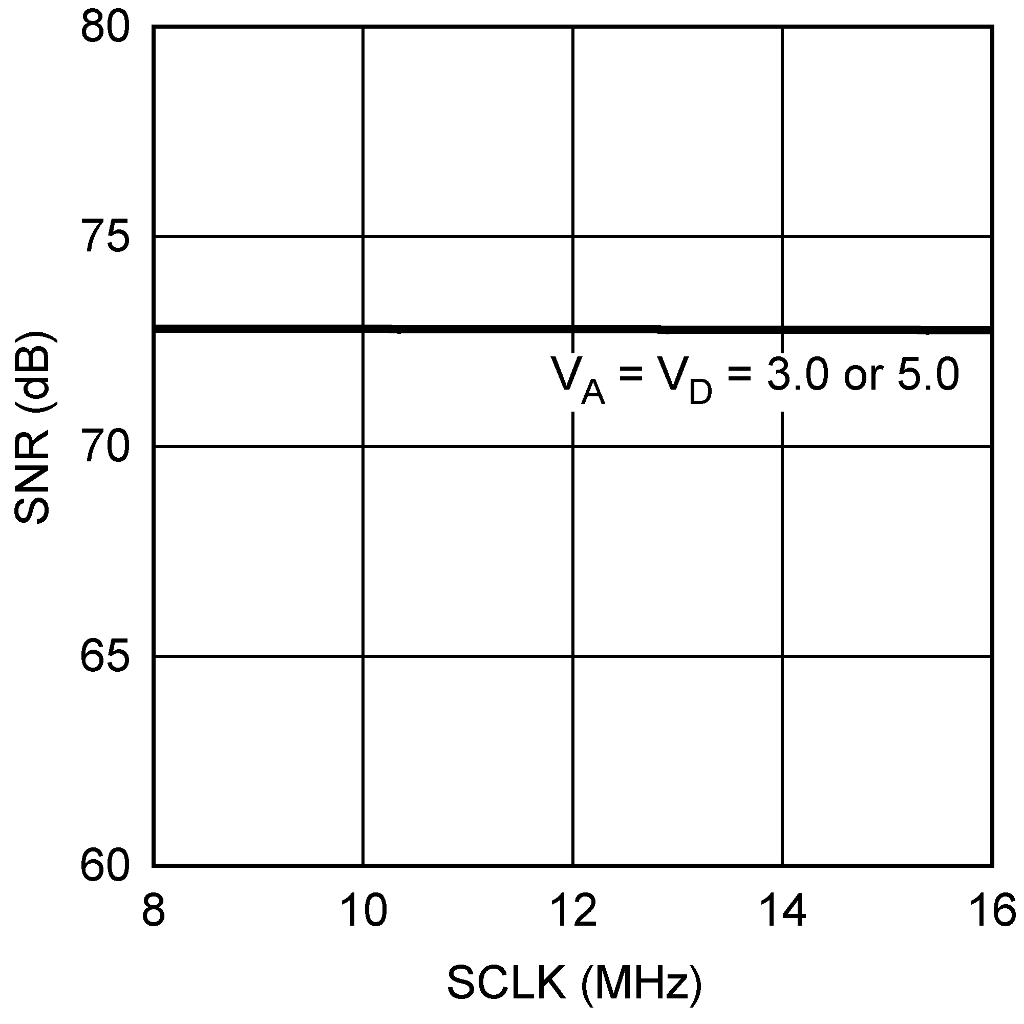 Figure 22. SNR vs. SCLK
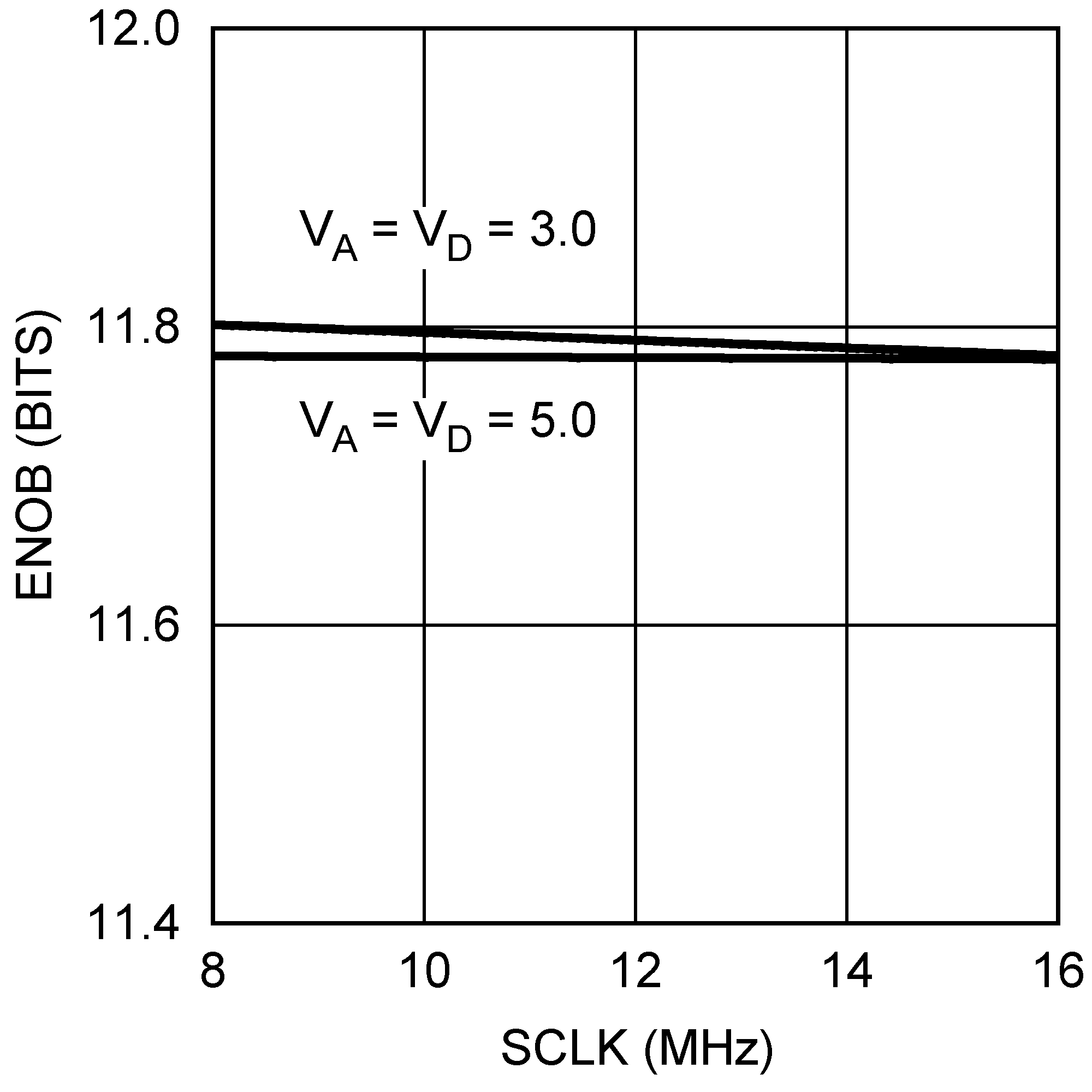 Figure 24. ENOB vs. SCLK
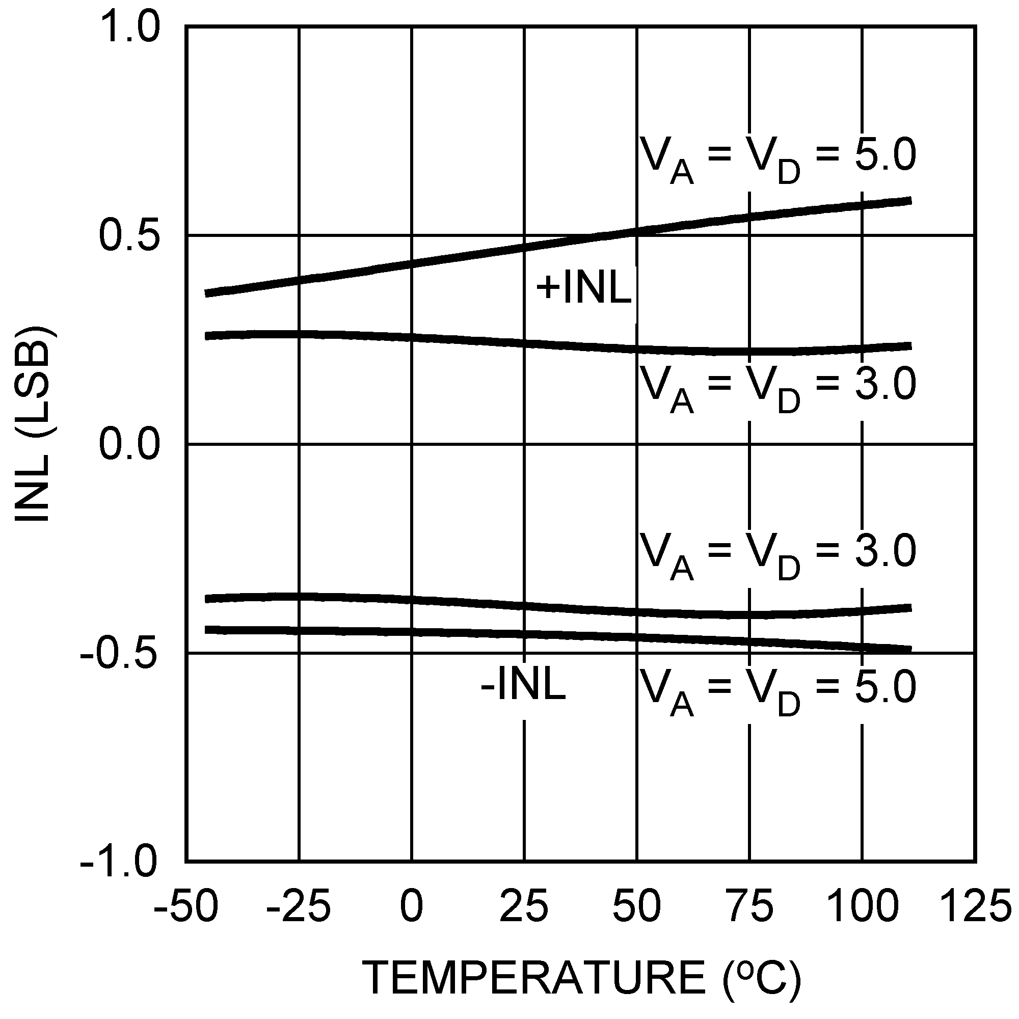 Figure 26. INL vs. Temperature
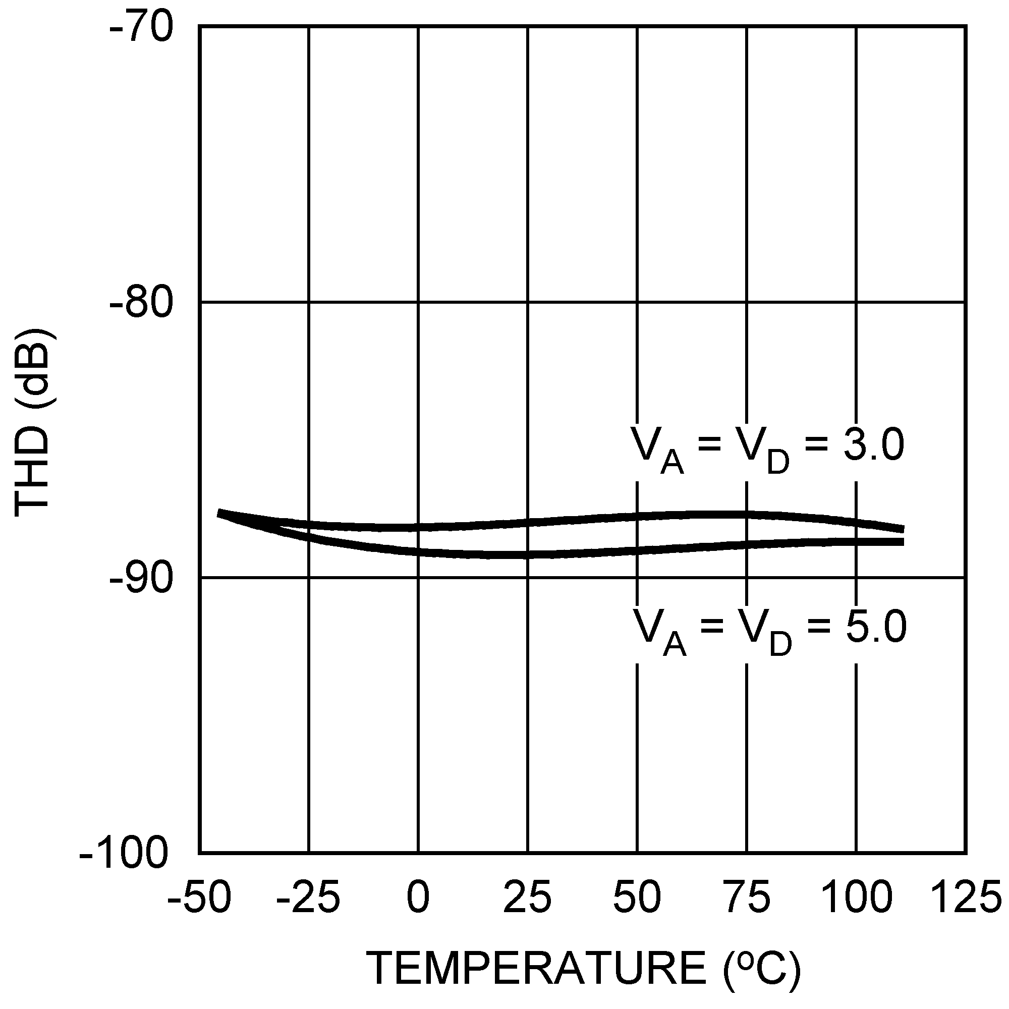 Figure 28. THD vs. Temperature
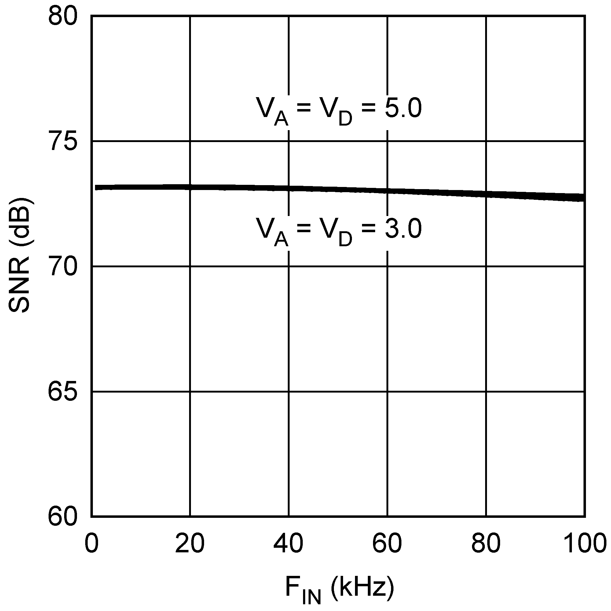 Figure 30. SNR vs. Input Frequency
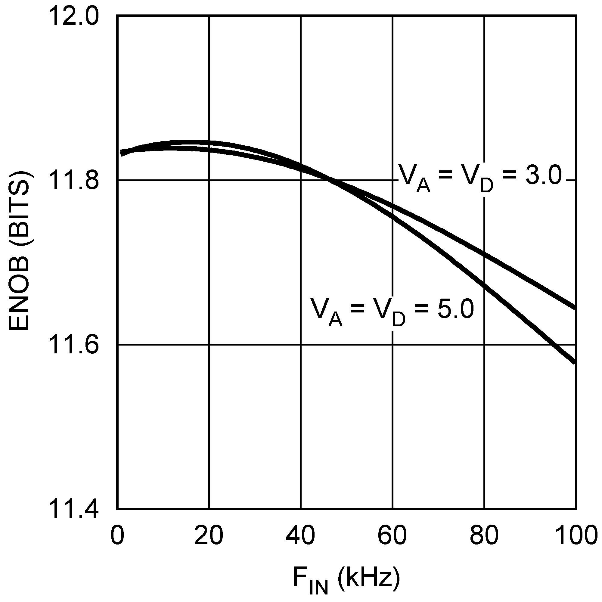 Figure 32. ENOB vs. Input Frequency
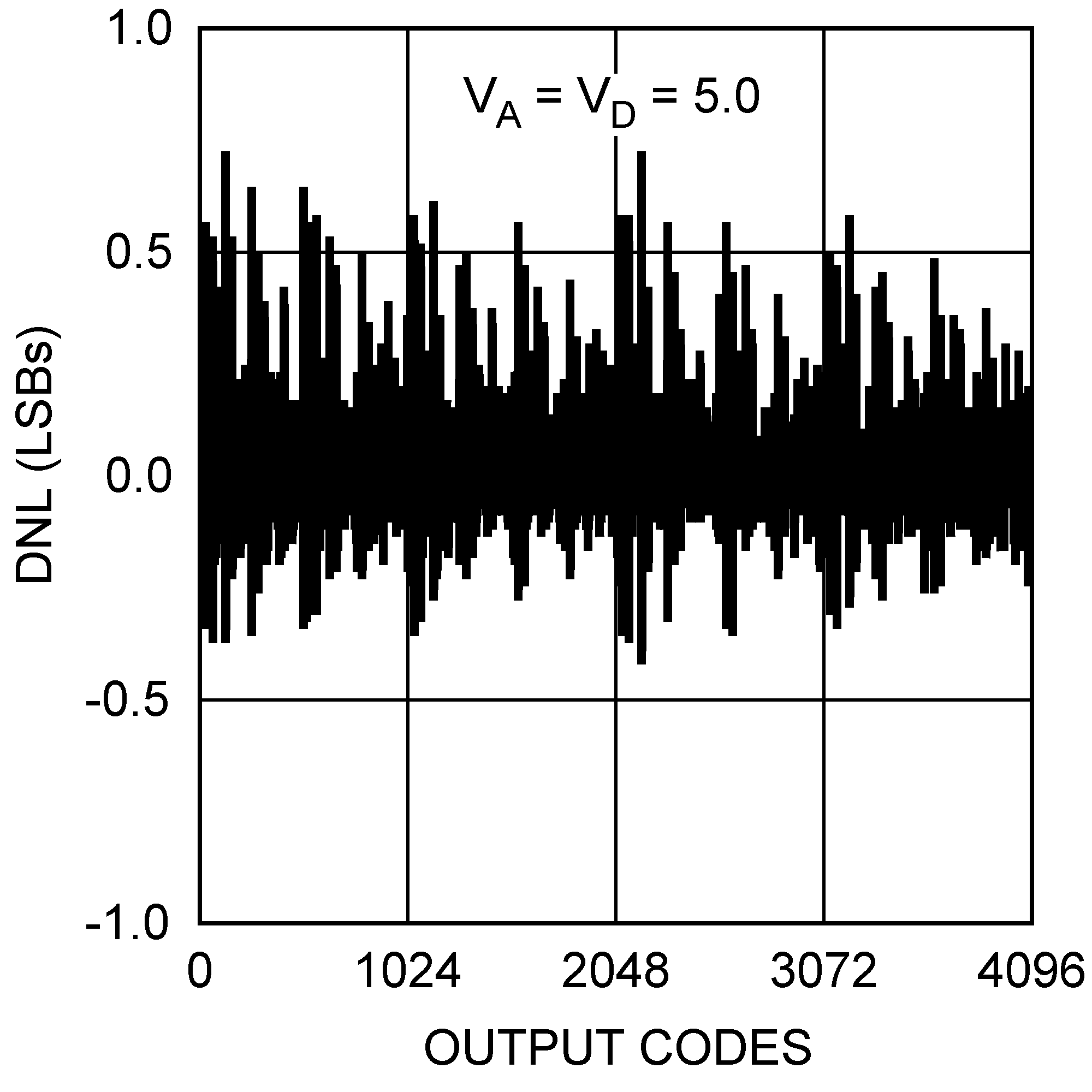 Figure 5. DNL
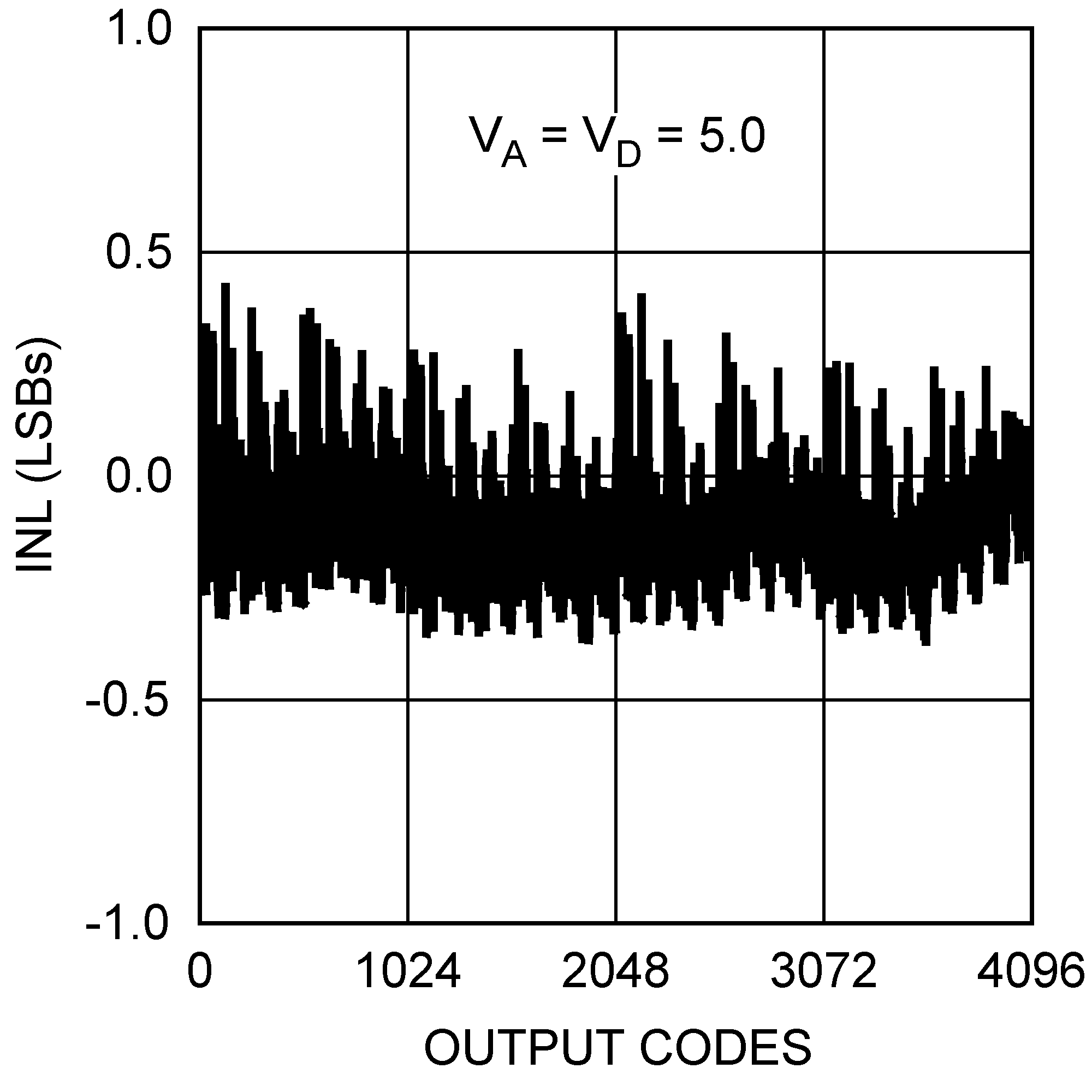 Figure 7. INL
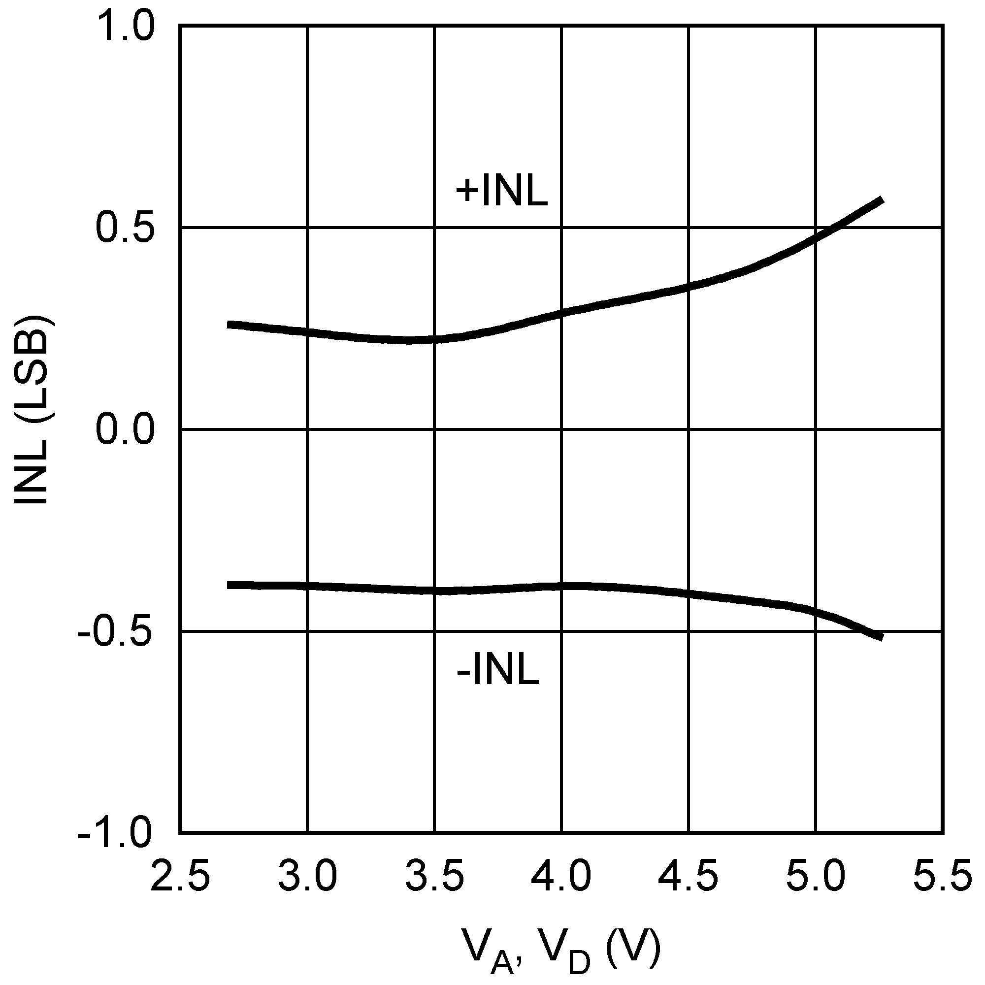 Figure 9. INL vs. Supply
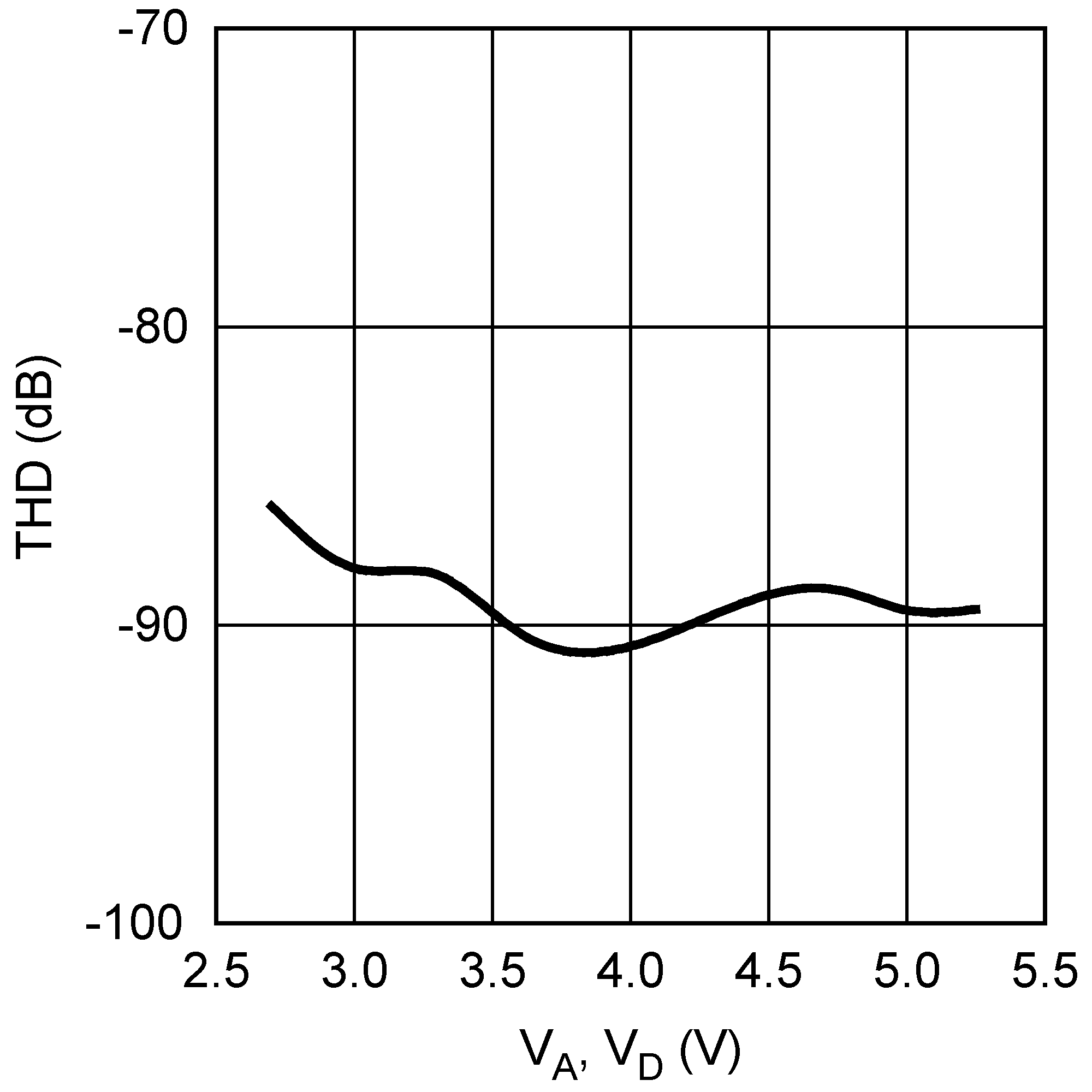 Figure 11. THD vs. Supply
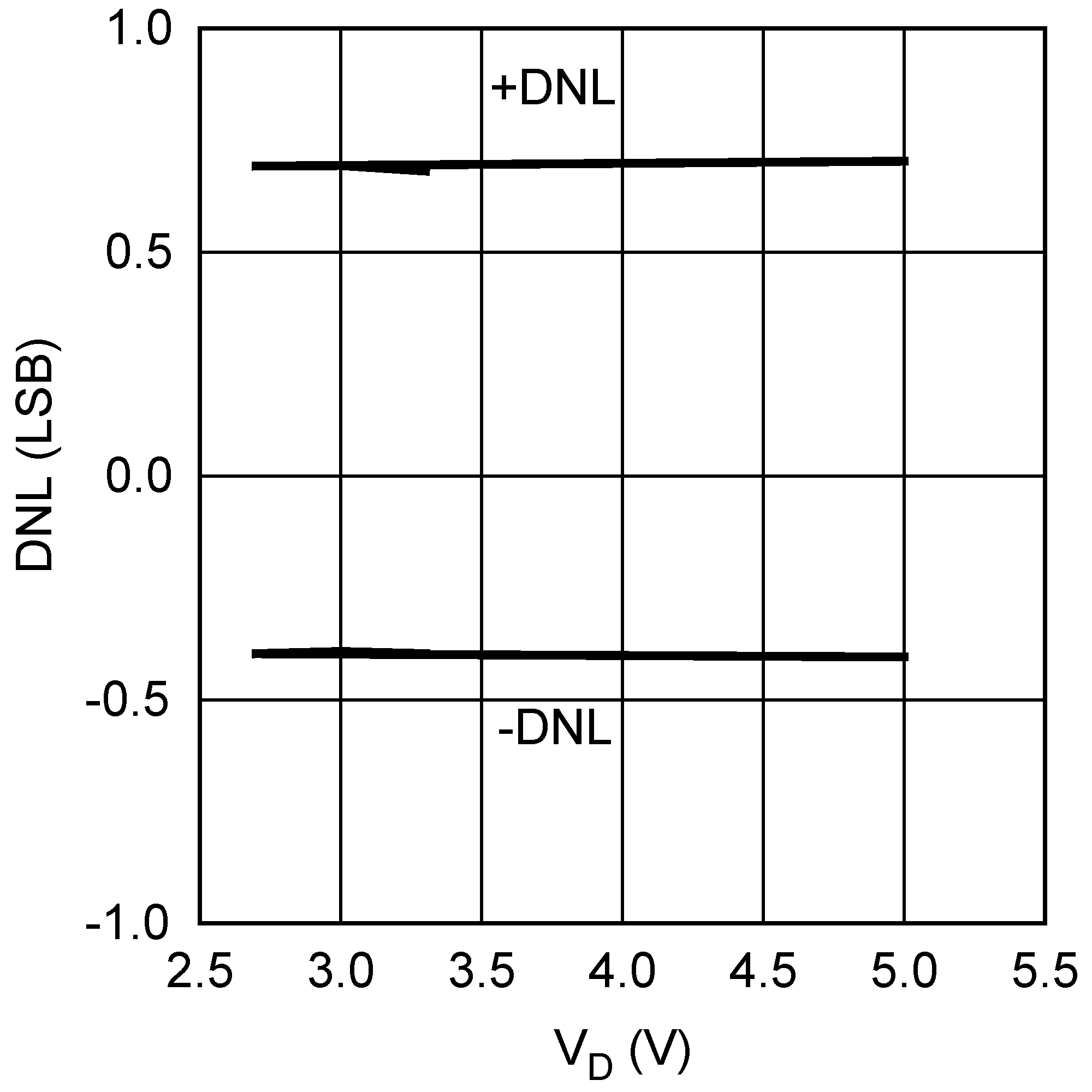 Figure 13. DNL vs. VD with VA = 5.0 V
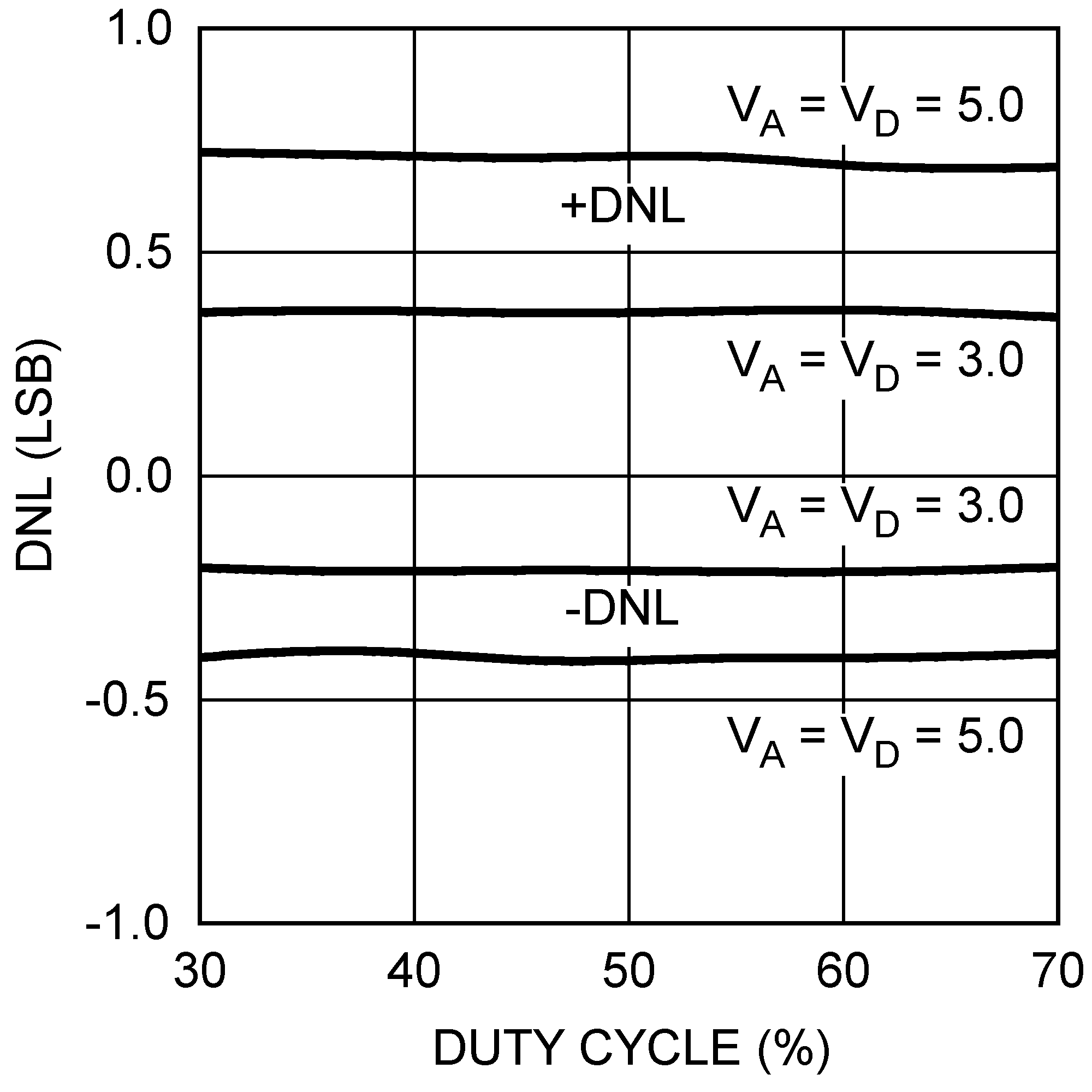 Figure 15. DNL vs. SCLK Duty Cycle
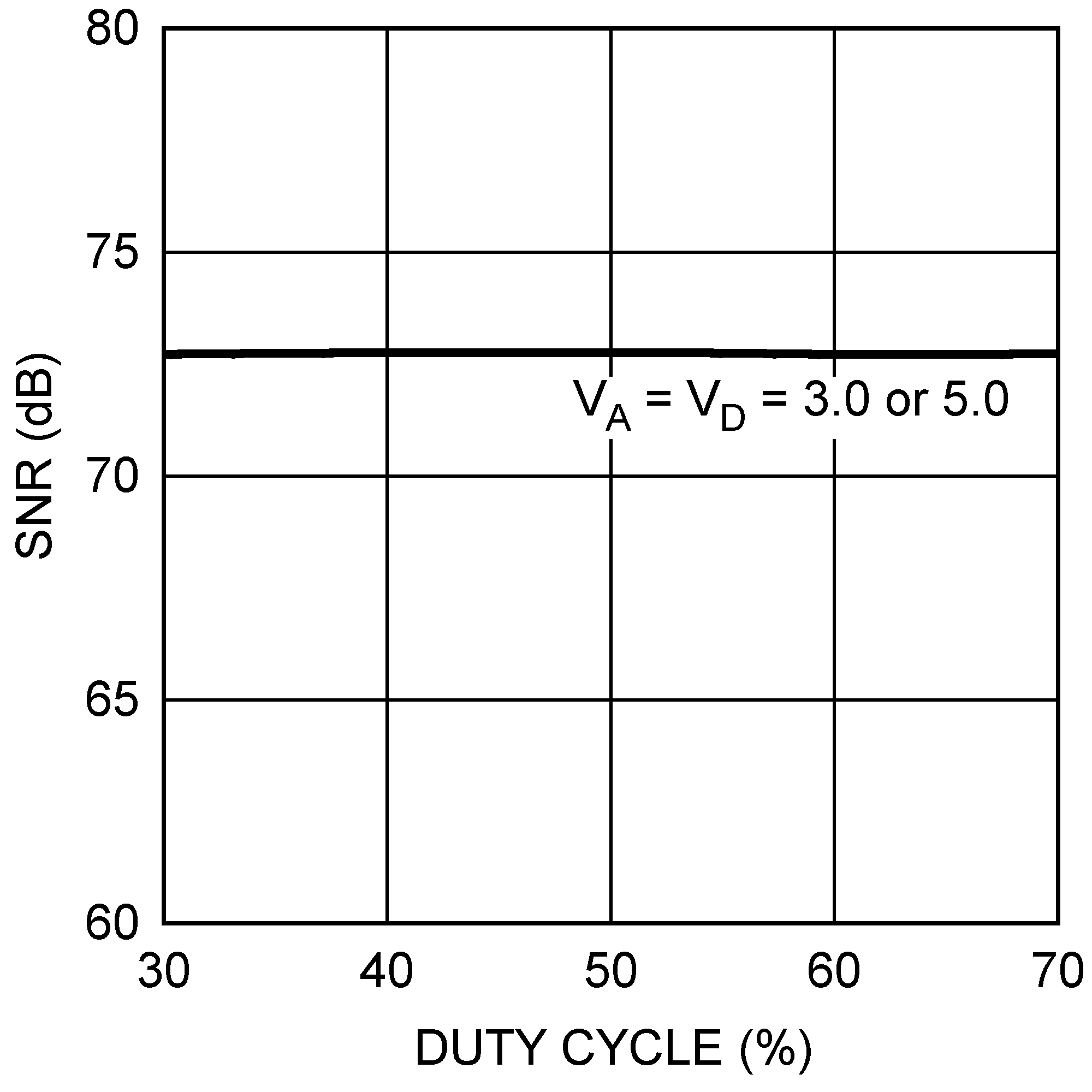 Figure 17. SNR vs. SCLK Duty Cycle
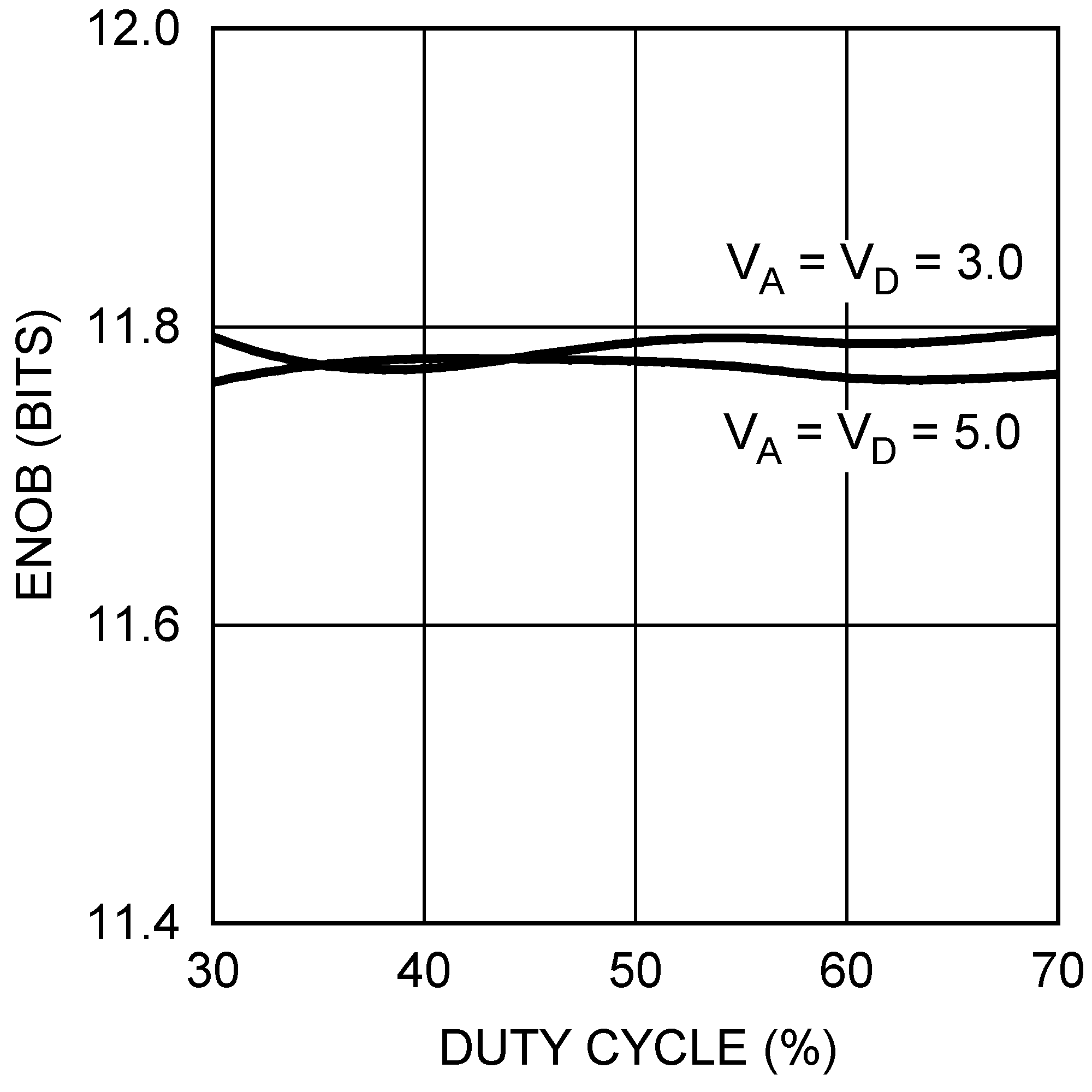 Figure 19. ENOB vs. SCLK Duty Cycle
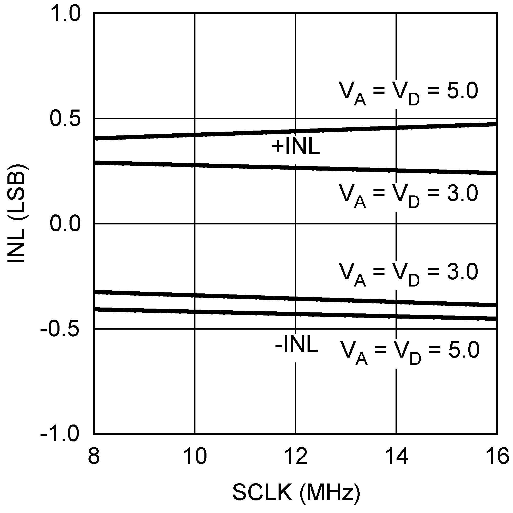 Figure 21. INL vs. SCLK
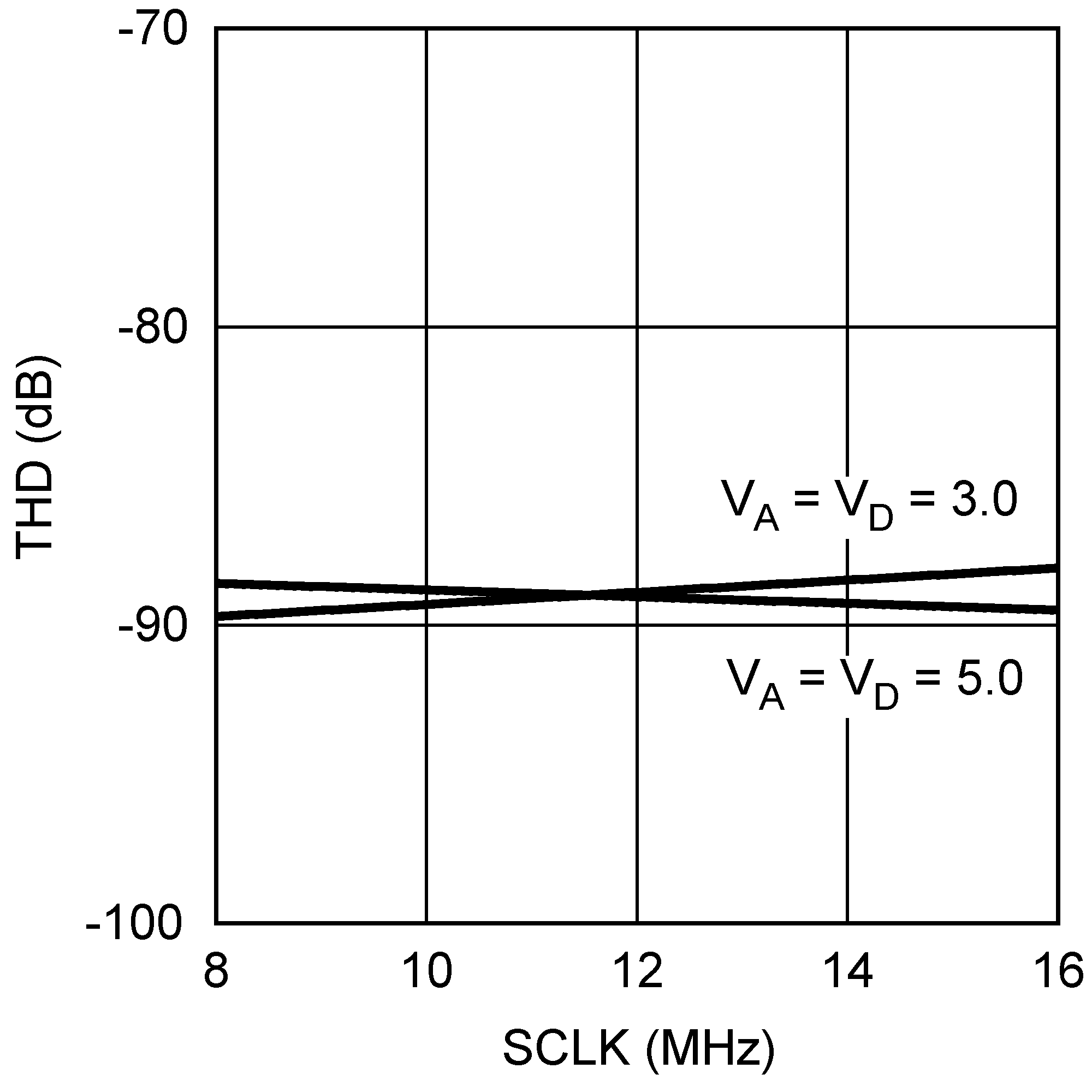 Figure 23. THD vs. SCLK
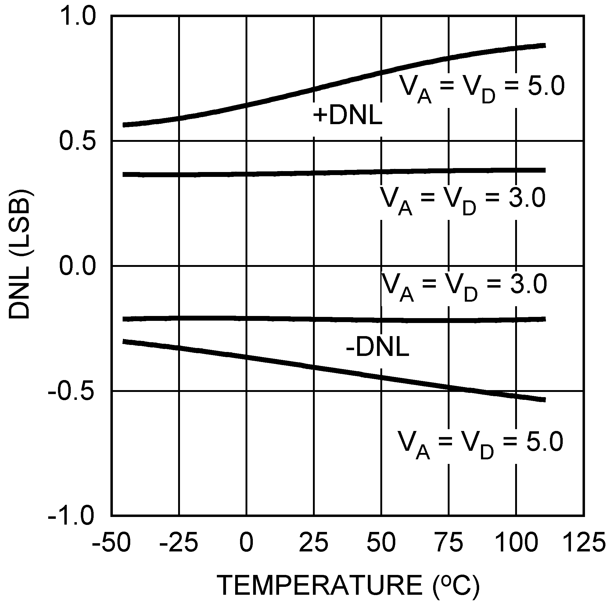 Figure 25. DNL vs. Temperature
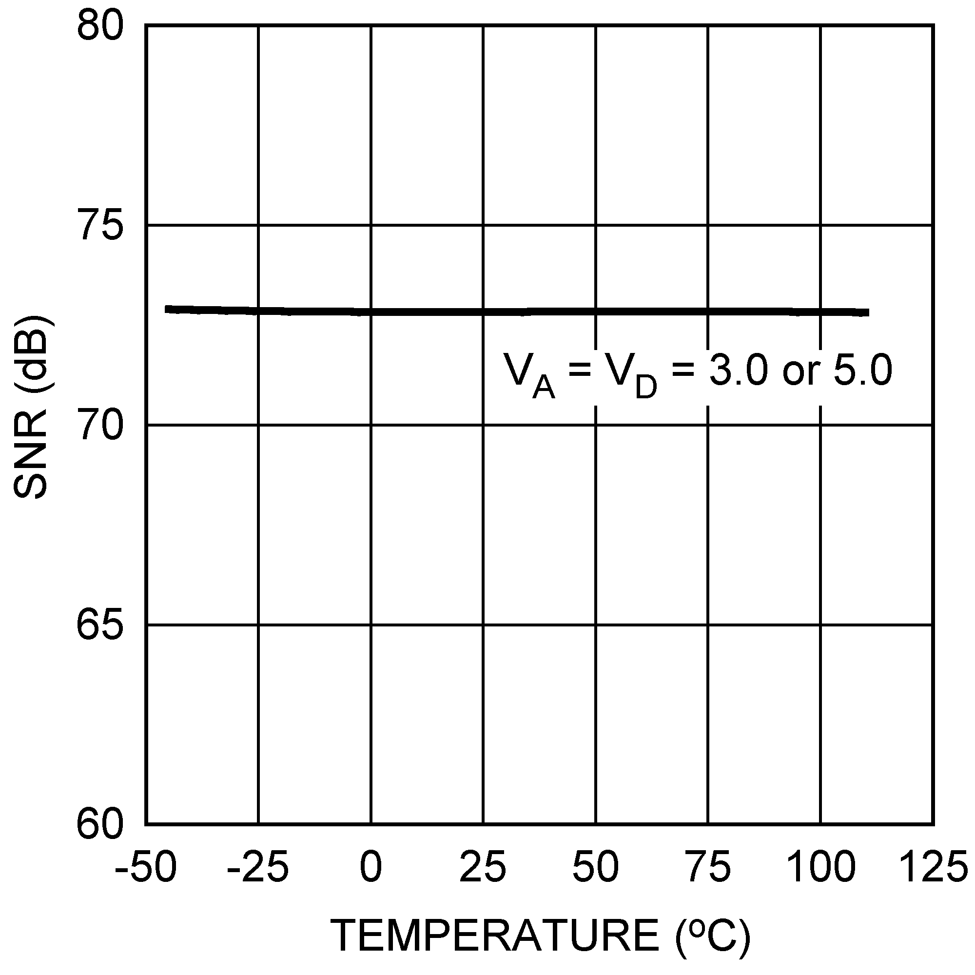 Figure 27. SNR vs. Temperature
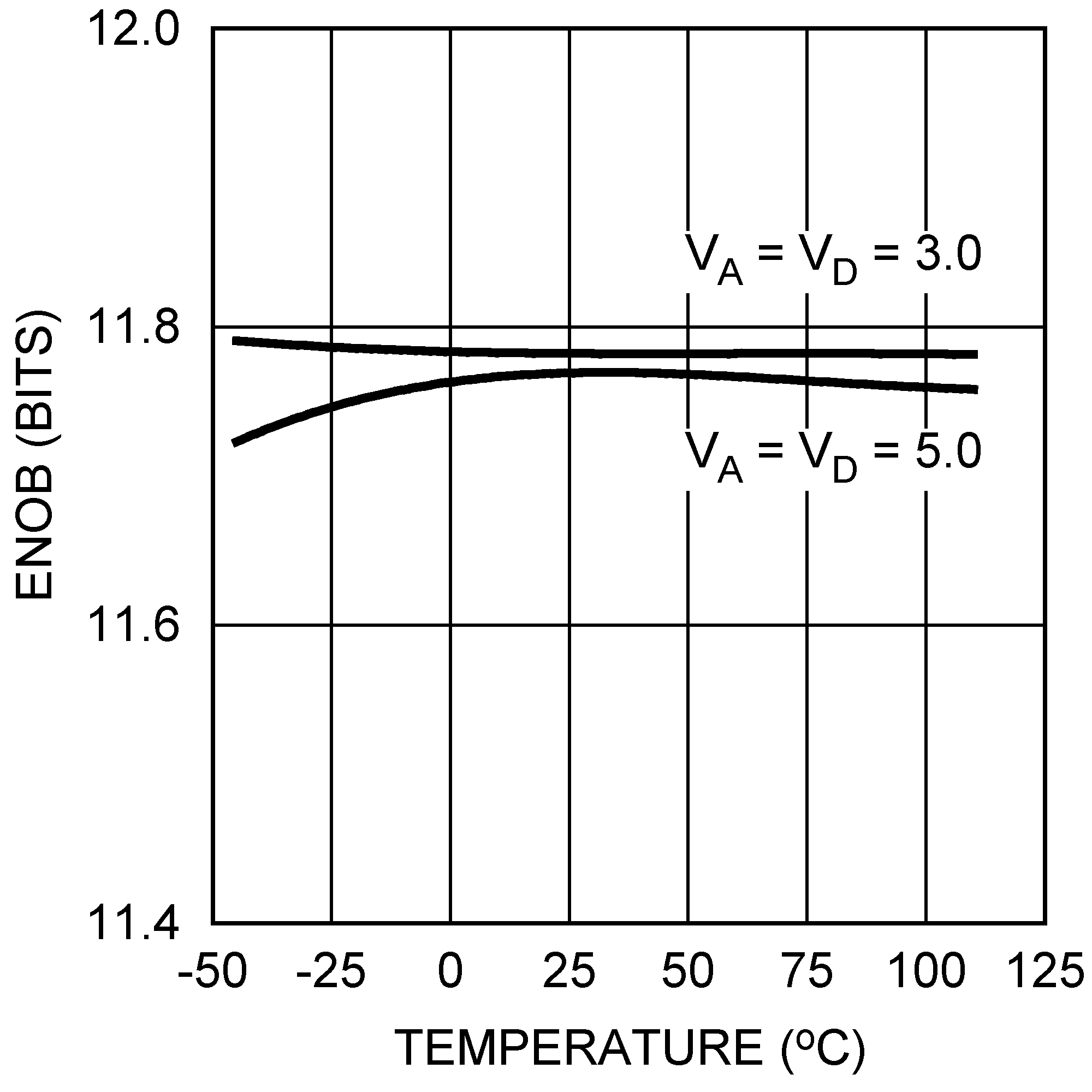 Figure 29. ENOB vs. Temperature
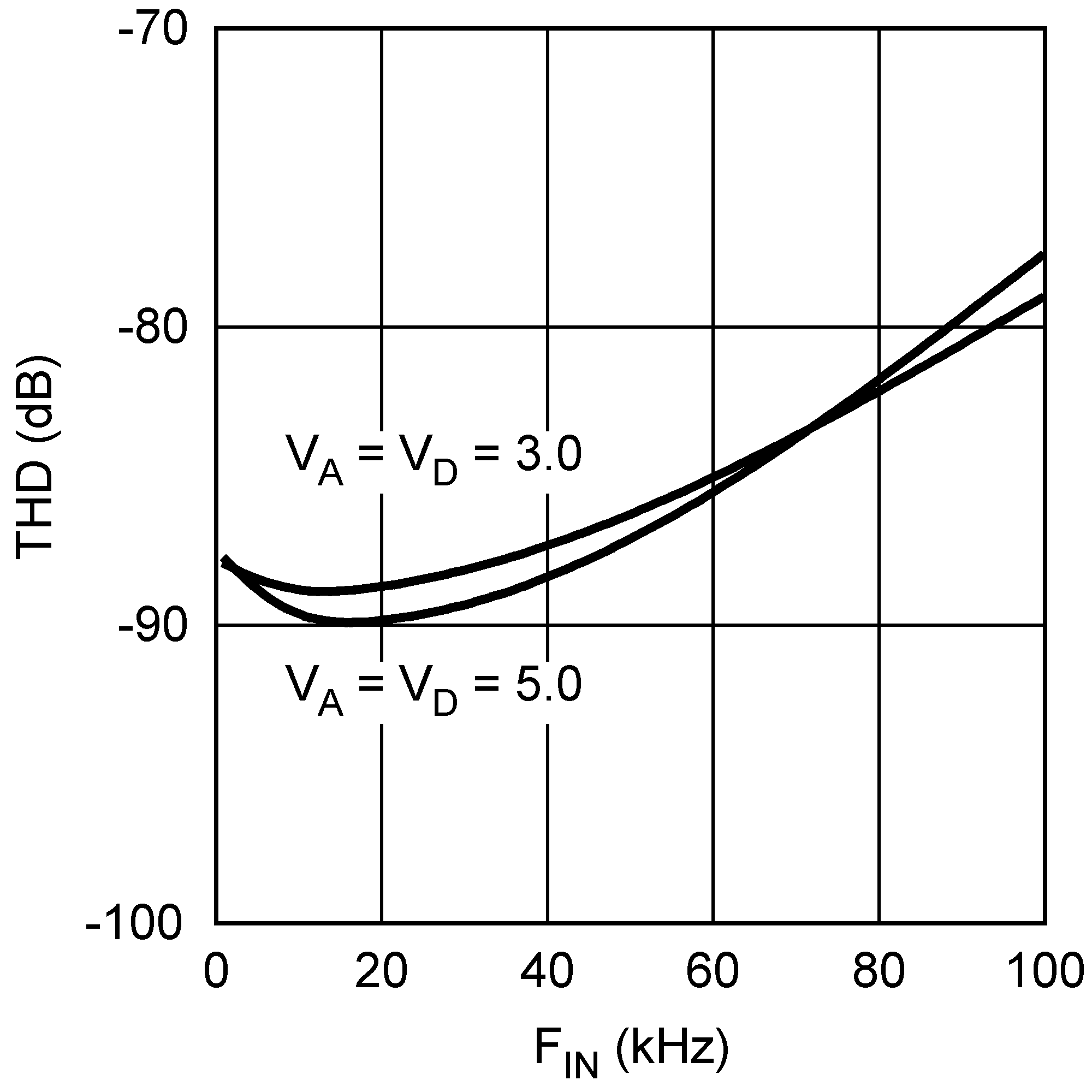 Figure 31. THD vs. Input Frequency
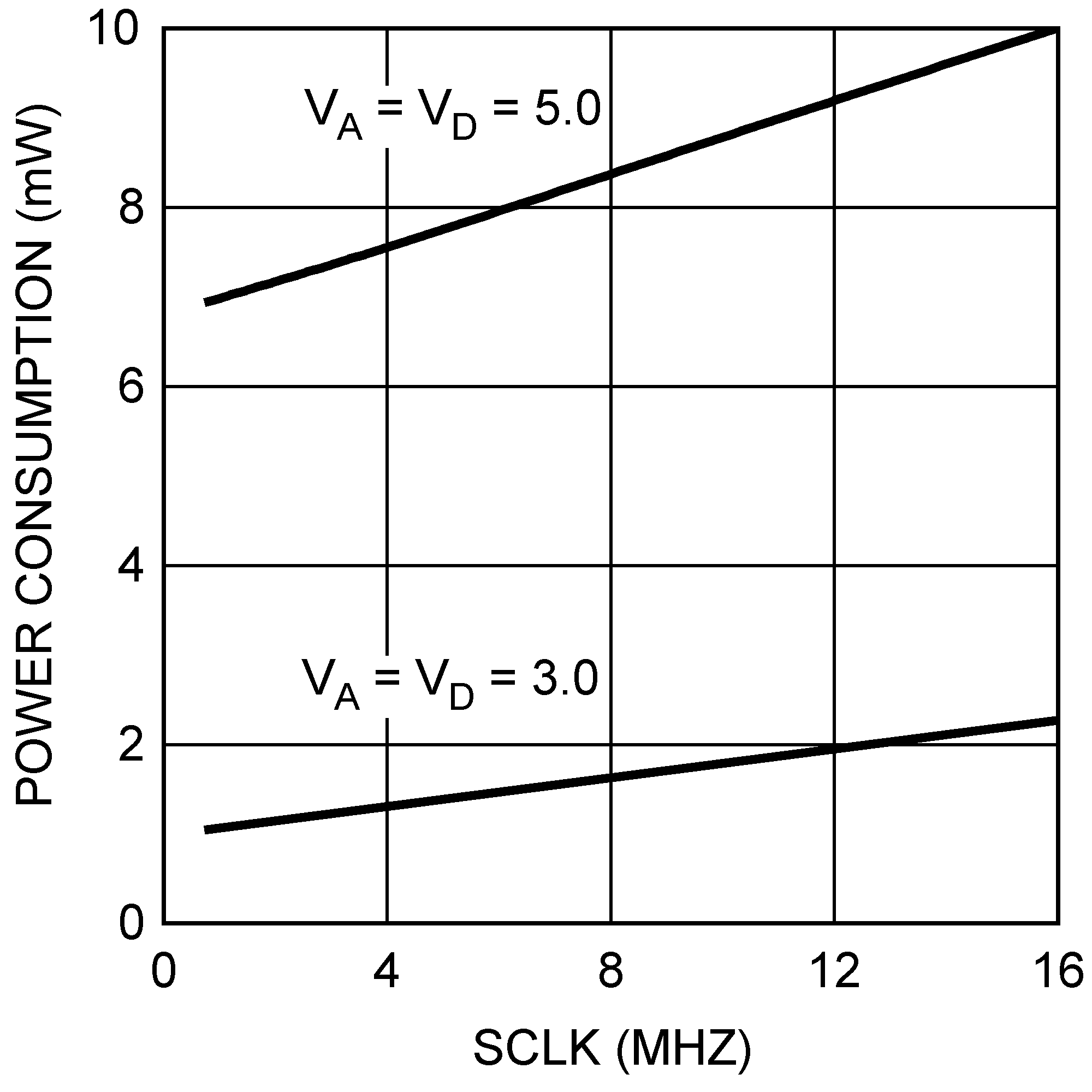 Figure 33. Power Consumption vs. SCLK