SNAS298G August 2005 – January 2015 ADC128S102
PRODUCTION DATA.
10 Layout
10.1 Layout Guidelines
Capacitive coupling between the noisy digital circuitry and the sensitive analog circuitry can lead to poor performance. The solution is to keep the analog circuitry separated from the digital circuitry and the clock line as short as possible.
Digital circuits create substantial supply and ground current transients. The logic noise generated could have significant impact upon system noise performance. To avoid performance degradation of the ADC128S102 due to supply noise, do not use the same supply for the ADC128S102 that is used for digital logic.
Generally, analog and digital lines should cross each other at 90° to avoid crosstalk. However, to maximize accuracy in high resolution systems, avoid crossing analog and digital lines altogether. It is important to keep clock lines as short as possible and isolated from ALL other lines, including other digital lines. In addition, the clock line should also be treated as a transmission line and be properly terminated.
The analog input should be isolated from noisy signal traces to avoid coupling of spurious signals into the input. Any external component (e.g., a filter capacitor) connected between the converter's input pins and ground or to the reference input pin and ground should be connected to a very clean point in the ground plane.
We recommend the use of a single, uniform ground plane and the use of split power planes. The power planes should be located within the same board layer. All analog circuitry (input amplifiers, filters, reference components, etc.) should be placed over the analog power plane. All digital circuitry and I/O lines should be placed over the digital power plane. Furthermore, all components in the reference circuitry and the input signal chain that are connected to ground should be connected together with short traces and enter the analog ground plane at a single, quiet point.
10.2 Layout Example
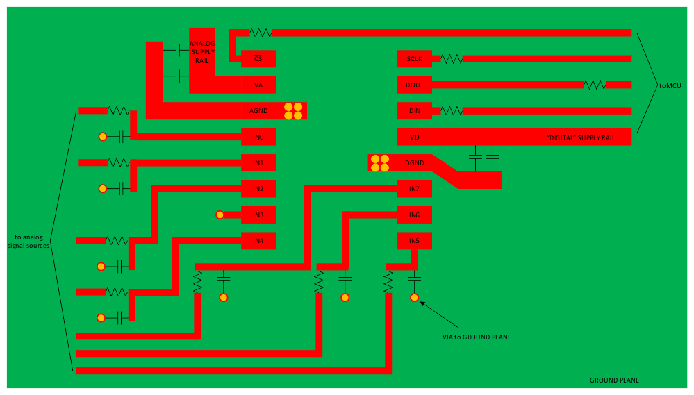 Figure 40. Layout Schematic