SCAS416Q March 1994 – September 2016 SN74ALVC164245
PRODUCTION DATA.
- 1 Features
- 2 Applications
- 3 Description
- 4 Revision History
- 5 Pin Configuration and Functions
-
6 Specifications
- 6.1 Absolute Maximum Ratings
- 6.2 ESD Ratings
- 6.3 Recommended Operating Conditions: VCCB at 3.3 V
- 6.4 Recommended Operating Conditions: VCCA at 2.5 V
- 6.5 Thermal Information
- 6.6 Electrical Characteristics: VCCA = 2.7 V to 3.6 V
- 6.7 Electrical Characteristics: VCCA = 2.3 V to 2.7 V
- 6.8 Switching Characteristics
- 6.9 Operating Characteristics
- 6.10 Typical Characteristics
- 7 Parameter Measurement Information
- 8 Detailed Description
- 9 Application and Implementation
- 10Power Supply Recommendations
- 11Layout
- 12Device and Documentation Support
- 13Mechanical, Packaging, and Orderable Information
1 Features
- Member of the Texas Instruments Widebus™ Family
- Maximum tpd of 5.8 ns at 3.3 V
- ±24-mA Output Drive at 3.3 V
- Control Inputs VIH/VIL Levels Are Referenced to VCCA Voltage
- Latch-Up Performance Exceeds 250 mA Per JESD 17
2 Applications
- Electronic Points of Sale
- Printers and Other Peripherals
- Motor Drives
- Wireless and Telecom Infrastructures
- Wearable Health and Fitness Devices
3 Description
This 16-bit (dual-octal) noninverting bus transceiver contains two separate supply rails. B port has VCCB, which is set to operate at 3.3 V and 5 V. A port has VCCA, which is set to operate at 2.5 V and 3.3 V. This allows for translation from a 2.5-V to a 3.3-V
environment, and vice versa, or from a 3.3-V to a 5-V environment, and vice versa.
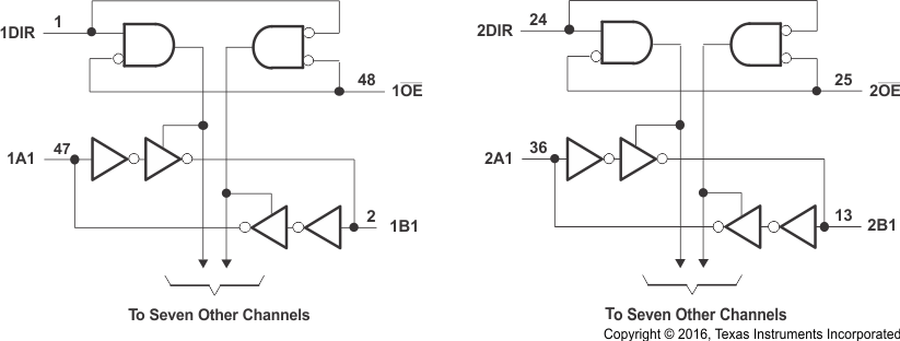
The SN74ALVC164245 is designed for asynchronous communication between data buses. The control circuitry (1DIR, 2DIR, 1OE, and 2OE) is powered by VCCA.
To ensure the high-impedance state during power up or power down, the output-enable (OE) input should be tied to VCC through a pullup resistor; the minimum value of the resistor is determined by the current-sinking capability of the driver.
The logic levels of the direction-control (DIR) input and the output-enable (OE) input activate either the B-port outputs or the A-port outputs or place both output ports into the high-impedance mode. The device transmits data from the A bus to the B bus when the B-port outputs are activated, and from the B bus to the A bus when the A-port outputs are activated. The input circuitry on both A and B ports always is active and must have a logic HIGH or LOW level applied to prevent excess ICC and ICCZ.
Device Information(1)
| PART NUMBER | PACKAGE | BODY SIZE (NOM) |
|---|---|---|
| SN74ALVC164245 | TSSOP (48) | 12.50 mm × 6.10 mm |
| SSOP (48) | 15.88 mm × 7.49 mm | |
| BGA MICROSTAR JUNIOR (56) | 7.00 mm × 4.50 mm | |
| BGA MICROSTAR JUNIOR (54) | 8.00 mm × 5.50 mm |
- For all available packages, see the orderable addendum at the end of the data sheet.
Logic Diagram (Positive Logic)
