SCLS418H June 1998 – December 2014 SN74AHCT367
PRODUCTION DATA.
- 1 Features
- 2 Applications
- 3 Description
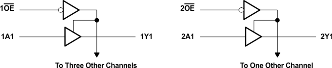
- 4 Simplified Schematic
- 5 Revision History
- 6 Pin Configuration and Functions
- 7 Specifications
- 8 Parameter Measurement Information
- 9 Detailed Description
- 10Application and Implementation
- 11Power Supply Recommendations
- 12Layout
- 13Mechanical, Packaging, and Orderable Information
封装选项
请参考 PDF 数据表获取器件具体的封装图。
机械数据 (封装 | 引脚)
- DB|16
- PW|16
- D|16
- DGV|16
散热焊盘机械数据 (封装 | 引脚)
- D|16
订购信息
1 Features
- Inputs are TTL-Voltage Compatible
- True Outputs
- Latch-Up Performance Exceeds 100 mA
Per JESD 78, Class II - ESD Protection Exceeds JESD 22
- 2000-V Human-Body Model
- 200-V Machine Model
- 2000-V Charged-Device Model
2 Applications
- Telecom Infrastructure
- TVs
- Set Top Boxes
- Network Switches
- Wireless Infrastructure
- Electronic Points of Sale
3 Description
The SN74AHCT367 device is designed specifically to improve both the performance and density of
3-state memory address drivers, clock drivers, and bus-oriented receivers and transmitters.
Device Information(1)
| PART NUMBER | PACKAGE | BODY SIZE (NOM) |
|---|---|---|
| SN74AHCT367 | PDIP (16) | 19.30 mm x 6.35 mm |
| SSOP (16) | 6.50 mm x 5.30 mm | |
| TSSOP (16) | 5.00 mm x 4.40 mm | |
| SOP (16) | 10.20 mm x 5.30 mm | |
| SOIC (16) | 9.00 mm x 3.90 mm |
- For all available packages, see the orderable addendum at the end of the data sheet.
4 Simplified Schematic