SNVSA38 November 2014 LM3281
PRODUCTION DATA.
- 1 Features
- 2 Applications
- 3 Description
- 4 Revision History
- 5 Pin Configuration and Functions
- 6 Specifications
- 7 Detailed Description
- 8 Application and Implementation
- 9 Power Supply Recommendations
- 10Layout
- 11Device and Documentation Support
- 12Mechanical, Packaging, and Orderable Information
1 Features
- Operates from a Single Li-Ion Cell (3 V to 5.5 V)
- 6-MHz (typ.) PWM Switching Frequency
- Fixed Output Voltage: 3.3 V
- Up to 1.2-A Maximum Load Capability
- High Efficiency: 94% (typ.) with 3.8-V VIN at 300 mA
- Analog Bypass: 60-mV (typ.) Drop-Out at 600 mA
- Low IQ: 16 µA typical, 25 µA maximum
- Automatic ECO/PWM/Bypass Mode Change
- Forced PWM Mode for Low Output-Voltage Ripple
- Soft-Start Limits Input Current on Start-Up
- Current Overload Protection
- Thermal Overload Protection
- Small Total Solution Size: < 7.5 mm2
2 Applications
- WLAN, WiFi Station Devices
- WiFi RF PC Cards
- Battery-Powered RF Devices
3 Description
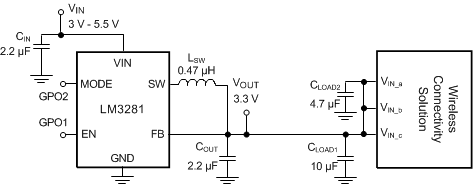
The LM3281 is a high-efficiency low-noise miniature DC-DC converter optimized for powering noise-sensitive wireless connectivity chipsets and RF Front End Modules (FEMs) from a single Lithium-Ion cell. The LM3281 is ideal for “always on” applications with very low unloaded quiescent current of 16 µA (typ.).
The LM3281 steps down an input supply voltage to a fixed output voltage of 3.3 V with output current up to 1200 mA. Five different modes of operation are used to optimize efficiency and minimize battery drain. In Pulse Width Modulation (PWM) mode, the device operates at a fixed frequency of 6 MHz which minimizes RF interference when driving medium-to-heavy loads. At light load, the device automatically enters into Economy (ECO) mode with reduced quiescent current. In a low-battery voltage condition, a bypass mode reduces the voltage dropout to 60 mV (typ.) at 600 mA. If very low output voltage ripple is desired at light loads, the device can also be forced into PWM mode. Shutdown mode turns the device off and reduces battery consumption to 0.1 μA (typ.).
Device Information(1)
| PART NUMBER | PACKAGE | BODY SIZE |
|---|---|---|
| LM3281 | DSBGA (6) | 1.465 mm x 1.190 (MAX) |
- For all available packages, see the orderable addendum at the end of the datasheet.
Simplified Schematic