SNVS729F September 2011 – August 2014 LM10506
PRODUCTION DATA.
- 1 Features
- 2 Applications
- 3 Description
- 4 Revision History
- 5 Device Comparison Table
- 6 Pin Configuration and Functions
-
7 Specifications
- 7.1 Absolute Maximum Ratings
- 7.2 Handling Ratings
- 7.3 Recommended Operating Conditions
- 7.4 Thermal Information
- 7.5 General Electrical Characteristics
- 7.6 Buck 1 Electrical Characteristics
- 7.7 Buck 2 Electrical Characteristics
- 7.8 Buck 3 Electrical Characteristics
- 7.9 LDO Electrical Characteristics
- 7.10 Comparators Electrical Characteristics
- 7.11 Typical Characteristics
-
8 Detailed Description
- 8.1 Functional Block Diagram
- 8.2 Feature Description
- 8.3 Device Functional Modes
- 8.4 Programming
-
9 Application and Implementation
- 9.1 Application Information
- 9.2 Typical Application
- 10Power Supply Recommendations
- 11Layout
- 12Device and Documentation Support
- 13Mechanical, Packaging, and Orderable Information
1 Features
- Three Highly Efficient Programmable Buck Regulators
- Buck Regulator Outputs:
- Buck 1: 1.1 V to 3.6 V; 1.3 A
- Buck 2: 1.1 V to 3.6 V; 400 mA
- Buck 3: 0.7 V to 1.335 V; 600 mA
- ±3% Feedback Voltage Accuracy
- Up to 95% Efficient Buck Regulators
- 2MHz Switching Frequency for Smaller Inductor Size
- Integrated FETs with Low RDSON
- Bucks Operate With Their Phases Shifted to Reduce the Input Current Ripple and Capacitor Size
- Programmable Output Voltage via the SPI™ Interface
- Overvoltage and Undervoltage Lockout
- Automatic Internal Soft Start With Power-On Reset
- Current Overload and Thermal Shutdown Protection
- Bypass Mode Available on Bucks 1 and 2
- PFM Mode for Low-Load, High-Efficiency Operation
- Buck Regulator Outputs:
- Low-Dropout LDO 3.2 V, 100 mA
- SPI-Programmable Interrupt Comparator (2 V to 4 V)
- Alternate Buck VOUT Selectable via H/L Logic Pins
- RESET, STANDBY Pins
2 Applications
Solid-State Drives
3 Description
The LM10506 is an advanced PMU containing three configurable, high-efficiency buck regulators for supplying variable voltages. The device is ideal for supporting ASIC and SOC designs for Solid-State and Flash drives.
The LM10506 operates cooperatively with ASIC to optimize the supply voltage for low-power conditions and Power Saving modes via the SPI interface. It also supports a 100-mA LDO and a programmable Interrupt Comparator.
Device Information(1)
| PART NUMBER | PACKAGE | BODY SIZE (MAX) |
|---|---|---|
| LM10506 | DSBGA (34) | 2.84 mm x 2.84 mm |
- For all available packages, see the orderable addendum at the end of the datasheet.
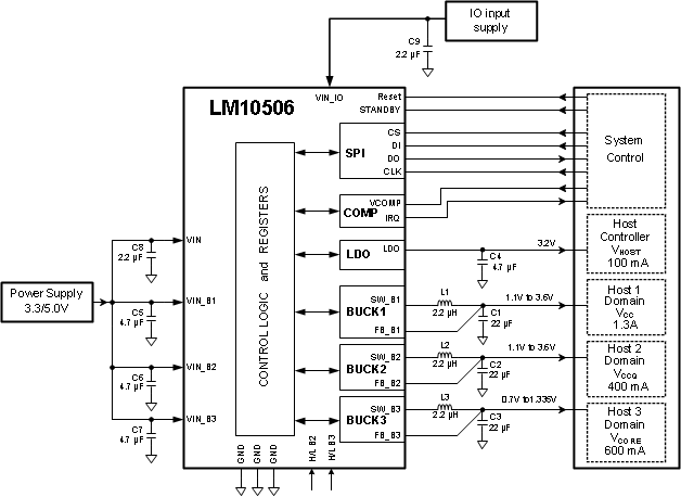
Simplified Schematic
4 Revision History
Changes from E Revision (March 2013) to F Revision
- Changed format to meet new TI standards; added Device Information and Handling Ratings tables; replace SUPPLY SPECIFICATION table with Device Comparison table, rename Functional Description and Applications sections, reformat and add new information, add Devices and Documentation section Go