ZHCS958G June 2012 – September 2017 BQ24392
PRODUCTION DATA.
8 Application and Implementation
NOTE
Information in the following applications sections is not part of the TI component specification, and TI does not warrant its accuracy or completeness. TI’s customers are responsible for determining suitability of components for their purposes. Customers should validate and test their design implementation to confirm system functionality.
8.1 Application Information
8.1.1 Using the BQ24392 GPIOs
8.1.1.1 CHG_AL and CHG_DET
The BQ24392 has 2 charger indicators, CHG_AL_N and CHG_DET, that the host can use to determine whether it can charge and if it can charge at a low or high current. Table 2 demonstrates how these outputs should be interpreted. CHG_AL_N is an open drain output and is active when the output of the pin is low. CHG_DET is a push-pull output and is high in the active state.
Table 2. bq24392 Outputs
| CHG_AL_N | CHG_DET | |
|---|---|---|
| High-Z | X | Charging is not allowed |
| Low | Low | Low-current charging is allowed |
| Low | High | High-current charging is allowed |
The system must define what is meant by low-current and high-current charging. If CHG_DET is high, a system could try to draw 2 A, 1.5 A, or 1.0 A. If the system is trying to support > 1.5-A chargers, then the system has to use a charger IC that is capable of monitoring the VBUS voltage as it tries to pull the higher current values. If the voltage on VBUS starts to drop because that high of a current is supported then the system has to reduce the amount of current it is trying to draw until it finds a stable state with VBUS not dropping.
8.1.1.2 SW_OPEN
SW_OPEN is an open drain output that indicates whether the USB switches are opened or closed. In the High-Z state the switches are open and in the active, or low state, the switches are closed. The host should monitor this pin to know when the switches are closed or open.
8.1.1.3 GOOD_BAT
GOOD_BAT is used by the host controller to indicate the status of the battery to the BQ24392. This pin affects the switch status for a SDP or CDP, and it also affects the Dead Battery Provision (DBP) timer as discussed in the Charger Detection section.
8.1.1.4 Slow Plug-in Event
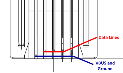
As you insert a charger into the USB receptacle, the pins are configured so that the VBUS and GND pins make contact first. This presents a problem as the BQ24392 (or any other charger detection IC) requires access to the D+ and D– lines to run detection. This is why the BQ24392 has a standard 130-ms debounce time after VBUS valid to run the detection algorithm. This delay helps minimize the effects of the D+ and D– lines making contact after VBUS and GND.
Figure 4 is from the datasheet of a standard male micro-USB connector and shows how the data connections (red line) are slightly recessed from the power connections (blue line).
 Figure 4. Data Connections Recessed from Power Connections
However, in some cases the charger is inserted very slowly, causing the VBUS and GND to make contact long before D+ and D–. Due to this effect, there is no guaranteed detection time as the detection time can vary based on how long it takes to insert the charger. If longer than 600 ms is taken to insert the charger into the USB receptacle, the detection algorithm of the BQ24392 will timeout and instead of the charger being detected as a DCP, it is now detected as a nonstandard charger (D+ and D– floating).
8.2 Typical Application
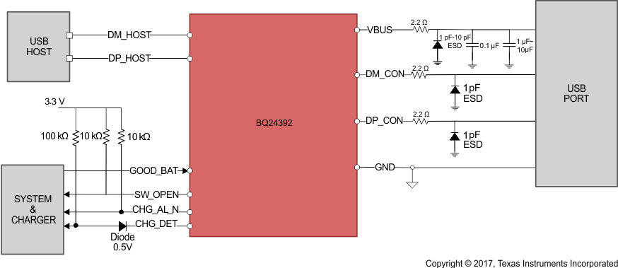
The BQ24392 device is used between the micro or mini-USB connector port and USB host to enable and disable the USB data path and detect chargers that are inserted into the micro or mini-USB connector.
 Figure 5. Application Schematic
8.2.1 Design Requirements
VBUS requires 1μF - 10μF and 0.1-μF bypass capacitors to reduce noise from circuit elements by providing a low impedance path to ground for the unwanted high frequency content. The 0.1-μF capacitor filters out higher frequencies and has a lower series inductance while the 1μF ~1 0μF capacitor filters out the lower frequencies and has a much higher series inductance. Using both capacitors will provide better load regulation across the frequency spectrum.
SW_OPEN and CHG_AL_N are open-drain outputs that require a 10-kΩ pull-up resistor to VDDIO.
VBUS, DM_CON, and DP_CON are recommended to have an external resistor of 2.2-Ω to provide extra ballasting to protect the chip and internal circuitry.
DM_CON and DP_CON are recommended to have a 1-pF external ESD protection diode rated for 8-kV IEC protection to prevent failure in case of an 8-kV IEC contact discharge.
VBUS is recommended to have a 1-pF ~ 10-pF external ESD Protection Diode rated for 8-kV IEC protection to prevent failure in case of an 8-kV IEC contact discharge
CHG_DET is a push-pull output pin. An external pull-up and diode are shown to depict a typical 3.3-V system. The pull-up resistor and diode are optional. The pull-up range on the CHG_DET pin is from 3.5 V to VVBUS. When VVBUS > 7 V, CHG_DET will be clamped to 7 V.
8.2.2 Detailed Design Procedure
The minimum pull-up resistance for the open-drain data lines is a function of the pull-up voltage VPU, output logic LOW voltage VOL(max), and Output logic LOW current IOL.
The maximum pull-up resistance for the open-drain data lines is a function of the maximum rise time of the desired signal, tr, and the bus capacitance, Cb.
8.2.3 Application Curves
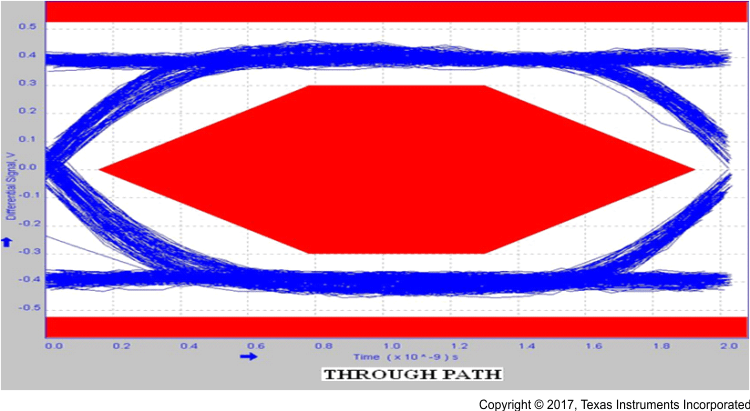
 Figure 6. 480-Mbps USB 2.0 Eye Diagram with No Device
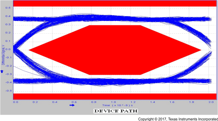
 Figure 7. 480-Mbps USB 2.0 Eye Diagram with USB Switch