SLOS358C September 2011 – April 2020 THS4531
PRODUCTION DATA.
- 1 Features
- 2 Applications
- 3 Description
- 4 Revision History
- 5 Packaging and Ordering Information
- 6 Electrical Specifications
- 7 Device Information
- 8 Table of Graphs
- 9 Typical Characteristics: VS = 2.7 V
- 10Typical Characteristics: VS = 5 V
-
11Application Information
- 11.1 Typical Characteristics Test Circuits
- 11.2
Application Circuits
- 11.2.1 Differential Input to Differential Output Amplifier
- 11.2.2 Single-Ended Input to Differential Output Amplifier
- 11.2.3 Differential Input to Single-Ended Output Amplifier
- 11.2.4 Input Common-Mode Voltage Range
- 11.2.5 Setting the Output Common-Mode Voltage
- 11.2.6 Single-Supply Operation
- 11.2.7 Low Power Applications and the Effects of Resistor Values on Bandwidth
- 11.2.8 Driving Capacitive Loads
- 11.2.9 Audio Performance
- 11.2.10 Audio On and Off Pop Performance
- 11.3 Audio ADC Driver Performance: THS4531 AND PCM4204 Combined Performance
- 11.4 SAR ADC Performance
- 11.5 EVM and Layout Recommendations
- 12Device and Documentation Support
- 13Mechanical, Packaging, and Orderable Information
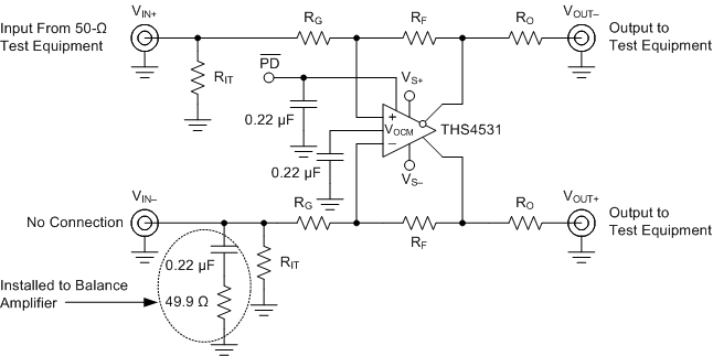
11.1.3 Slew Rate, Transient Response, Settling Time, Overdrive, Output Voltage, and Turn-On and Turn-Off Time
The circuit shown in Figure 68 is used to measure slew rate, transient response, settling time, overdrive recovery, and output voltage swing. Turn-on and turn-off times are measured with 50 Ω input termination on the PD input, by replacing the 0.22 µF capacitor with 49.9 Ω resistor.
 Figure 68. Slew Rate, Transient Response, Settling Time, ZO, Overdrive Recovery, VOUT Swing, and Turn-On and Trun-Off Test Circuit