ZHCSDJ8A March 2015 – April 2015 UCD3138A
PRODUCTION DATA.
- 1器件概述
- 2修订历史记录
- 3Device Comparison
- 4Terminal Configuration and Functions
- 5Specifications
-
6Detailed Description
- 6.1 Overview
- 6.2 ARM Processor
- 6.3 Memory
- 6.4 System Module
- 6.5 DPWM Modes of Operation
- 6.6 Sync FET Ramp and IDE Calculation
- 6.7 Automatic Mode Switching
- 6.8 DPWMC, Edge Generation, IntraMux
- 6.9 Filter
- 6.10 Communication Ports
- 6.11 Miscellaneous Analog
- 6.12 Package ID Information
- 6.13 Brownout
- 6.14 Global I/O
- 6.15 Temperature Sensor Control
- 6.16 I/O Mux Control
- 6.17 Current Sharing Control
- 6.18 Temperature Reference
-
7Application, Implementation, and Layout
- 7.1 Application Information
- 7.2 Typical Application
- 7.3 Layout
- 7.4 Power Supply Decoupling and Bulk Capacitors
- 8器件和文档支持
- 9机械封装和可订购信息
封装选项
机械数据 (封装 | 引脚)
散热焊盘机械数据 (封装 | 引脚)
订购信息
6 Detailed Description
6.1 Overview
The UCD3138A family is a digital power supply controller from Texas Instruments offering superior levels of integration and performance in a single chip solution. The UCD3138, in comparison to Texas Instruments UCD3138A digital power controller offers 32 kB of program Flash memory. The flexible nature of the UCD3138A family makes it suitable for a wide variety of power conversion applications.
In addition, multiple peripherals inside the device have been specifically optimized to enhance the performance of AC/DC and isolated DC/DC applications and reduce the solution component count in the IT and network infrastructure space. The UCD3138A family is a fully programmable solution offering customers complete control of their application, along with ample ability to differentiate their solution. At the same time, TI is committed to simplifying our customer’s development effort through offering best in class development tools, including application firmware, Code Composer StudioTM software development environment, and TI’s Fusion Power Development GUI which enables customers to configure and monitor key system parameters.
6.2 ARM Processor
The ARM7TDMI-S processor is a synthesizable member of the ARM family of general purpose 32-bit microprocessors. The ARM architecture is based on RISC (Reduced Instruction Set Computer) principles where two instruction sets are available. The 32-bit ARM instruction set and the 16-bit Thumb instruction set. The Thumb instruction allows for higher code density equivalent to a 16-bit microprocessor, with the performance of the 32-bit microprocessor.
The three-staged pipelined ARM processor has fetch, decode and execute stage architecture. Major blocks in the ARM processor include a 32-bit ALU, 32 x 8 multiplier, and a barrel shifter.
6.3 Memory
The UCD3138A (ARM7TDMI-S) is a Von-Neumann architecture, where a single bus provides access to all of the memory modules. All of the memory module addresses are sequentially aligned along the same address range. This applies to program flash, data flash, ROM and all other peripherals.
Within the UCD3138A architecture, there is a Boot ROM that contains the initial firmware startup routines for PMBUS communication and non-volatile (FLASH) memory download. This boot ROM is executed after power-up-reset checks if there is a valid FLASH program written. If a valid program is present, the ROM code branches to the main FLASH-program execution.
UCD3138A also supports customization of the boot program by allowing an alternative boot routine to be executed from program FLASH. This feature enables assignment of a unique address to each device; therefore, enabling firmware reprogramming even when several devices are connected on the same communication bus.
Two separate FLASH memory areas are present inside the device. The 32 kB Program FLASH is organized as an 8 k x 32 bit memory block and is intended to be for the firmware program. The block is configured with page erase capability for erasing blocks as small as 1kB per page, or with a mass erase for erasing the entire program FLASH array. The FLASH endurance is specified at 1000 erase/write cycles and the data retention is good for 100 years. The 2 kB data FLASH array is organized as a 512 x 32 bit memory (32 byte page size). The Data FLASH is intended for firmware data value storage and data logging. Thus, the Data FLASH is specified as a high endurance memory of 20 k cycles with embedded error correction code (ECC).
For run time data storage and scratchpad memory, a 4 kB RAM is available. The RAM is organized as a 1 k x 32 bit array.
6.3.1 CPU Memory Map and Interrupts
When the device comes out of power-on-reset, the data memories are mapped to the processor as follows:
6.3.1.1 Memory Map (After Reset Operation)
| Address | Size | Module |
|---|---|---|
| 0x0000_0000 – 0x0000_FFFF In 16 repeated blocks of 4K each |
16 X 4K | Boot ROM |
| 0x0001_0000 – 0x0001_7FFF | 32K | Program flash |
| 0x0001_8800 – 0x0001_8FFF | 2K | Data flash |
| 0x0001_9000 – 0x0001_9FFF | 4K | Data RAM |
6.3.1.2 Memory Map (Normal Operation)
Just before the boot ROM program gives control to FLASH program, the ROM configures the memory as follows:
| Address | Size | Module |
|---|---|---|
| 0x0000_0000 – 0x0000_7FFF | 32K | Program flash |
| 0x0001_0000 – 0x0001_AFFF | 4K | Boot ROM |
| 0x0001_8800 – 0x0001_8FFF | 2K | Data flash |
| 0x0001_9000 – 0x0001_9FFF | 4K | Data RAM |
6.3.1.3 Memory Map (System and Peripherals Blocks)
| Address | Size | Module |
|---|---|---|
| 0x0002_0000 - 0x0002_00FF | 256 | Loop Mux |
| 0x0003_0000 - 0x0003_00FF | 256 | Fault Mux |
| 0x0004_0000 - 0x0004_00FF | 256 | ADC |
| 0x0005_0000 - 0x0005_00FF | 256 | DPWM 3 |
| 0x0006_0000 - 0x0006_00FF | 256 | Filter 2 |
| 0x0007_0000 - 0x0007_00FF | 256 | DPWM 2 |
| 0x0008_0000 - 0x0008_00FF | 256 | Front End/Ramp I/F 2 |
| 0x0009_0000 - 0x0009_00FF | 256 | Filter 1 |
| 0x000A_0000 - 0x000A_00FF | 256 | DPWM 1 |
| 0x000B_0000 – 0x000B_00FF | 256 | Front End/Ramp I/F 1 |
| 0x000C_0000 - 0x000C_00FF | 256 | Filter 0 |
| 0x000D_0000 - 0x000D_00FF | 256 | DPWM 0 |
| 0x000E_0000 - 0x000E_00FF | 256 | Front End/Ramp I/F 0 |
| 0xFFF7_EC00 - 0xFFF7_ECFF | 256 | UART 0 |
| 0xFFF7_ED00 - 0xFFF7_EDFF | 256 | UART 1 |
| 0xFFF7_F000 - 0xFFF7_F0FF | 256 | Miscellaneous Analog Control |
| 0xFFF7_F600 - 0xFFF7_F6FF | 256 | PMBus Interface |
| 0xFFF7_FA00 - 0xFFF7_FAFF | 256 | GIO |
| 0xFFF7_FD00 - 0xFFF7_FDFF | 256 | Timer |
| 0xFFFF_FD00 - 0xFFFF_FDFF | 256 | MMC |
| 0xFFFF_FE00 - 0xFFFF_FEFF | 256 | DEC |
| 0xFFFF_FF20 - 0xFFFF_FF37 | 23 | CIM |
| 0xFFFF_FF40 - 0xFFFF_FF50 | 16 | PSA |
| 0xFFFF_FFD0 - 0xFFFF_FFEC | 28 | SYS |
The registers and bit definitions inside the system and peripheral blocks are detailed in the programmer’s guide for each peripheral.
6.3.2 Boot ROM
The UCD3138A incorporates a 4k boot ROM. This boot ROM includes support for:
- Program download through the PMBus
- Device initialization
- Examining and modifying registers and memory
- Verifying and executing program FLASH automatically
- Jumping to a customer defined boot program
The Boot ROM is entered automatically on device reset. It initializes the device and then performs checksums on the Program FLASH. If the first 2 kB of program FLASH has a valid checksum, the program jumps to location 0 in the Program FLASH. This permits the use of a customer boot program. If the first checksum fails, it performs a checksum on the complete 32 kB of program flash. If this is valid, it also jumps to location 0 in the program flash. This permits full automated program memory checking, when there is no need for a custom boot program.
If neither checksum is valid, the Boot ROM stays in control, and accepts commands via the PMBus interface
These functions can be used to read and write to all memory locations in the UCD3138. Typically they are used to download a program to Program Flash, and to command its execution
6.3.3 Customer Boot Program
As described above, it is possible to generate a user boot program using 2 kB or more of the program flash. This can support things which the Boot ROM does not support, including:
- Program download via UART – useful especially for applications where the UCD3138A is isolated from the host (for example, PFC)
- Encrypted download – useful for code security in field updates.
6.3.4 Flash Management
The UCD3138A offers a variety of features providing for easy prototyping and easy flash programming. At the same time, high levels of security are possible for production code, even with field updates. Standard firmware will be provided for storing multiple copies of system parameters in data flash. This is minimizes the risk of losing information if programming is interrupted.
6.4 System Module
The System Module contains the interface logic and configuration registers to control and configure all the memory, peripherals and interrupt mechanisms. The blocks inside the system module are the address decoder, memory management controller, system management unit, central interrupt unit, and clock control unit.
6.4.1 Address Decoder (DEC)
The Address Decoder generates the memory selects for the FLASH, ROM and RAM arrays. The memory map addresses are selectable through configurable register settings. These memory selects can be configured from 1 kB to 16 MB. Power on reset uses the default addresses in the memory map for ROM execution, which is then configured by the ROM code to the application setup. During access to the DEC registers, a wait state is asserted to the CPU. DEC registers are only writable in the ARM privilege mode for user mode protection.
6.4.2 Memory Management Controller (MMC)
The MMC manages the interface to the peripherals by controlling the interface bus for extending the read and write accesses to each peripheral. The unit generates eight peripheral select lines with 1 kB of address space decoding.
6.4.3 System Management (SYS)
The SYS unit contains the software access protection by configuring user privilege levels to memory or peripherals modules. It contains the ability to generate fault or reset conditions on decoding of illegal address or access conditions. A clock control setup for the processor clock (MCLK) speed, is also available.
6.4.4 Central Interrupt Module (CIM)
The CIM accepts 32 interrupt requests for meeting firmware timing requirements. The ARM processor supports two interrupt levels: FIQ and IRQ. FIQ is the highest priority interrupt. The CIM provides hardware expansion of interrupts by use of FIQ/IRQ vector registers for providing the offset index in a vector table. This numerical index value indicates the highest precedence channel with a pending interrupt and is used to locate the interrupt vector address from the interrupt vector table. Interrupt channel 0 has the lowest precedence and interrupt channel 31 has the highest precedence. To remove the interrupt request, the firmware should clear the request as the first action in the interrupt service routine. The request channels are maskable, allowing individual channels to be selectively disabled or enabled.
Table 6-1 Interrupt Priority Table
6.5 DPWM Modes of Operation
The DPWM is a complex logic system which is highly configurable to support several different power supply topologies. The discussion below will focus primarily on waveforms, timing and register settings, rather than on logic design.
The DPWM is centered on a period counter, which counts up from 0 to PRD, and then is reset and starts over again.
The DPWM logic causes transitions in many digital signals when the period counter hits the target value for that signal.
6.5.1 Normal Mode
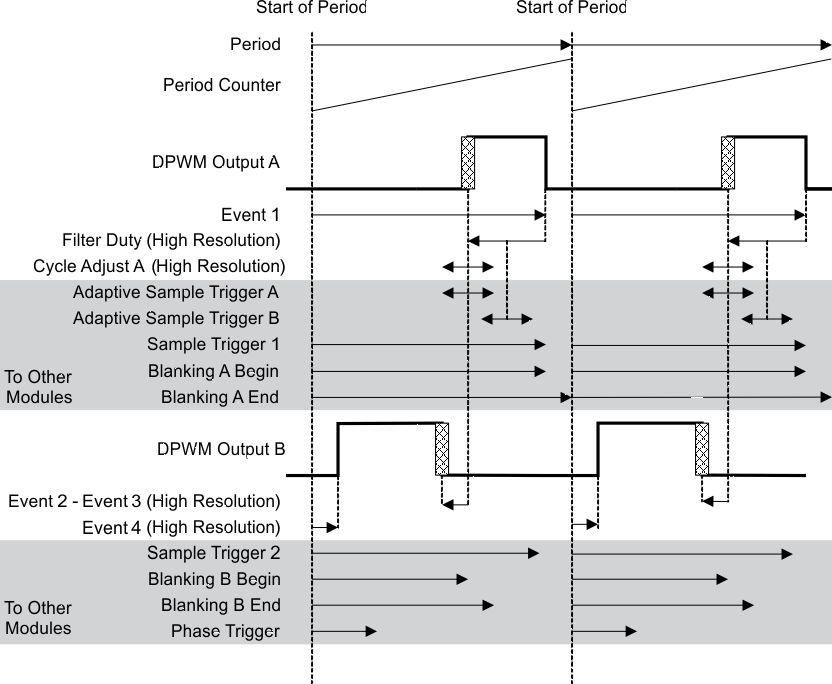
In Normal mode, the Filter output determines the pulse width on DPWM A. DPWM B fits into the rest of the switching period, with a dead time separating it from the DPWM A on-time. It is useful for buck topologies. The drawing of the Normal Mode waveforms is shown in Figure 6-1.
Cycle adjust A can be used to adjust pulse widths on individual phases of a multi-phase system. This can be used for functions like current balancing. The Adaptive Sample Triggers can be used to sample in the middle of the on-time (for an average output), or at the end of the on-time (to minimize phase delay) The Adaptive Sample Register provides an offset from the center of the on-time. This can compensate for external delays, such as MOSFET and gate driver turn on times.
Blanking A-Begin and Blanking A-End can be used to blank out noise from the MOSFET turn on at the beginning of the period (DPWMA rising edge). Blanking B could be used at the turn off time of DPWMB. The other edges are dynamic, so blanking is more difficult.
Cycle Adjust B has no effect in Normal Mode.
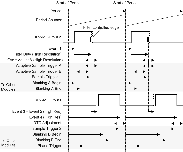
- DPWM A Rising Edge = Event 1
- DPWM A Falling Edge = Event 1 + Filter Duty + Cycle Adjust A
- Adaptive Sample Trigger A = Event 1 + Filter Duty + Adaptive Sample Register or
- Adaptive Sample Trigger B = Event 1 + Filter Duty/2 + Adaptive Sample Register
- DPWM B Rising Edge = Event 1 + Filter Duty + Cycle Adjust A + (Event 3 – Event 2)
- DPWM B Falling Edge = Event 4 + DTC Adjustment
- Phase Trigger = Phase Trigger Register value or Filter Duty
Events always set by their registers, regardless of mode:
- Sample Trigger 1, Sample Trigger 2, Blanking A Begin, Blanking A End, Blanking B
- Begin, Blanking B End
6.5.2 DPWM Multiple Output Mode
Multi mode is used for systems where each phase has only one driver signal. It enables each DPWM peripheral to drive two phases with the same pulse width, but with a time offset between the phases, and with different cycle adjusts for each phase.
The diagram for Multi-Mode is shown in Figure 6-2.
Event 2 and Event 4 are not relevant in Multi mode.
DPWMB can cross over the period boundary safely, and still have the proper pulse width, so full 100% pulse width operation is possible. DPWMA cannot cross over the period boundary.
Since the rising edge on DPWM B is also fixed, Blanking B-Begin and Blanking B-End can be used for blanking this rising edge.
Cycle Adjust B is usable on DPWM B.
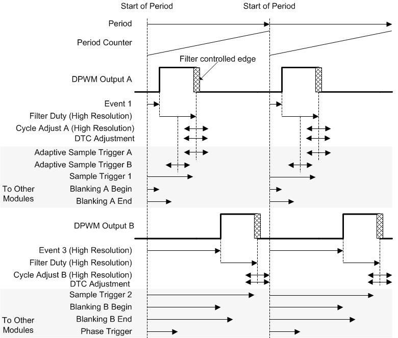
- DPWM A Rising Edge = Event 1
- DPWM A Falling Edge = Event 1 + Filter Duty + Cycle Adjust A + DTC Adjustment
- Adaptive Sample Trigger A = Event 1 + Filter Duty + Adaptive Sample Register or
- Adaptive Sample Trigger B = Event 1 + Filter Duty/2 + Adaptive Sample Register
- DPWM B Rising Edge = Event 3
- DPWM B Falling Edge = Event 3 + Filter Duty + Cycle Adjust B + DTC Adjustment
- Phase Trigger = Phase Trigger Register value or Filter Duty
Events always set by their registers, regardless of mode:
- Sample Trigger 1, Sample Trigger 2, Blanking A Begin, Blanking A End, Blanking B
- Begin, Blanking B End
6.5.3 DPWM Resonant Mode
This mode provides a symmetrical waveform where DPWMA and DPWMB have the same pulse width. As the switching frequency changes, the dead times between the pulses remain the same.
The equations for this mode are designed for a smooth transition from PWM mode to resonant mode, as described in Section 6.7.2. The diagram of this mode is shown in Figure 6-3.
The Filter has two outputs, Filter Duty and Filter Period. In this case, the Filter is configured so that the Filter Period is twice the Filter Duty. So if there were no dead times, each DPWM pin would be on for half of the period. For dead time handling, the average of the two dead times is subtracted from the Filter Duty for both DPWM pins. Therefore, both pins will have the same on-time, and the dead times will be fixed regardless of the period. The only edge which is fixed relative to the start of the period is the rising edge of DPWM A. This is the only edge for which the blanking signals can be used easily.
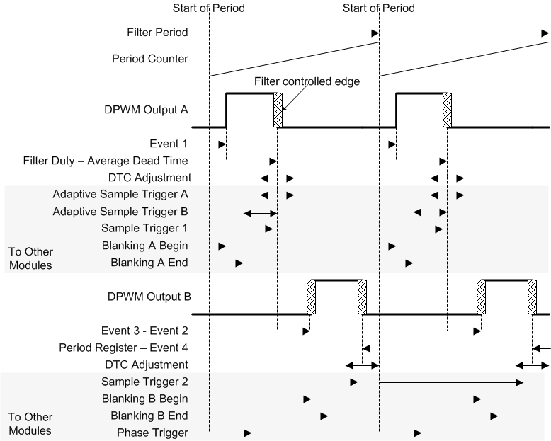
- Dead Time 1 = Event 3 - Event 2
- Dead Time 2 = Event 1 + Period Register - Event 4
- Average Dead Time = (Dead Time 1 + Dead Time 2)/2
- DPWM A Rising Edge = Event 1
- DPWM A Falling Edge = Event 1 + Filter Duty - Average Dead Time + DTC Adjustment
- Adaptive Sample Trigger A = Event 1 + Filter Duty + Adaptive Sample Register or
- Adaptive Sample Trigger B = Event 1 + Filter Duty/2 + Adaptive Sample Register
- DPWM B Rising Edge = Event 1 + Filter Duty - Average Dead Time + (Event 3 - Event 2)
- DPWM B Falling Edge = Filter Period - (Period Register - Event 4) + DTC Adjustment
- Phase Trigger = Phase Trigger Register value or Filter Duty
Events always set by their registers, regardless of mode:
- Sample Trigger 1, Sample Trigger 2, Blanking A Begin, Blanking A End, Blanking B
- Begin, Blanking B End
6.5.4 Triangular Mode
Triangular mode provides a stable phase shift in interleaved PFC and similar topologies. In this case, the PWM pulse is centered in the middle of the period, rather than starting at one end or the other. In Triangular Mode, only DPWM-B is available. The diagram for Triangular Mode is shown in Figure 6-4.
All edges are dynamic in triangular mode, so fixed blanking is not that useful. The adaptive sample trigger is not needed. It is very easy to put a fixed sample trigger exactly in the center of the FET on-time, because the center of the on-time does not move in this mode.
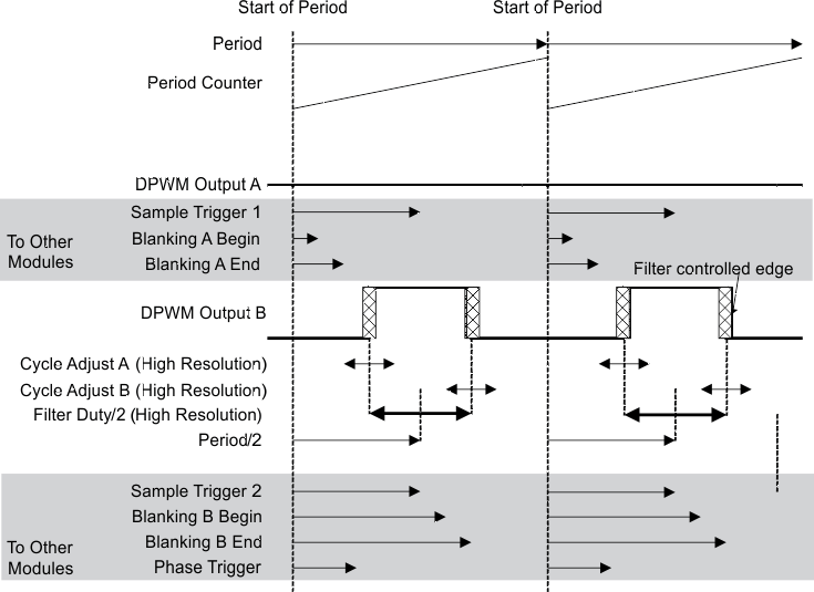
- DPWM A Rising Edge = None
- DPWM A Falling Edge = None
- Adaptive Sample Trigger = None
- DPWM B Rising Edge = Period / 2 - Filter Duty / 2 + Cycle Adjust A
- DPWM B Falling Edge = Period / 2 + Filter Duty / 2 + Cycle Adjust B
- Phase Trigger = Phase Trigger Register value or Filter Duty
Events always set by their registers, regardless of mode:
- Sample Trigger 1, Sample Trigger 2, Blanking A Begin, Blanking A End, Blanking B
- Begin, Blanking B End
6.5.5 Leading Edge Mode
Leading edge mode is very similar to Normal mode, reversed in time. The DPWM A falling edge is fixed, and the rising edge moves to the left, or backwards in time, as the filter output increases. The DPWM B falling edge stays ahead of the DPWMA rising edge by a fixed dead time. The diagram of the Leading Edge Mode is shown in Figure 6-5.
As in the Normal mode, the two edges in the middle of the period are dynamic, so the fixed blanking intervals are mainly useful for the edges at the beginning and end of the period.
- DPWM A Rising Edge = Event 1
- DPWM A Falling Edge = = Event 1 - Filter Duty + Cycle Adjust A
- Adaptive Sample Trigger A = Event 1 - Filter Duty + Adaptive Sample Register or
- Adaptive Sample Trigger B = Event 1 - Filter Duty / 2 + Adaptive Sample Register
- DPWM B Rising Edge = Event 4
- DPWM B Falling Edge = Event 1 - Filter Duty + Cycle Adjust A - ( Event 2 – Event 3 )
- Phase Trigger = Phase Trigger Register value or Filter Duty
Events always set by their registers, regardless of mode:
- Sample Trigger 1, Sample Trigger 2, Blanking A Begin, Blanking A End, Blanking B
- Begin, Blanking B End
6.6 Sync FET Ramp and IDE Calculation
The UCD3138A has built in logic for controlling MOSFETs for synchronous rectification (Sync FETs). This comes in two forms:
- Sync FET ramp
- Ideal Diode Emulation (IDE) calculation
When starting up a power supply, sometimes there is already a voltage on the output – this is called prebias. It is difficult to calculate the ideal Sync FET on-time for this case. If it is not calculated correctly, it may pull down the prebias voltage, causing the power supply to sink current.
To avoid this, Sync FETs are not turned on until the power supply has ramped up to the nominal voltage. The Sync FETs are turned on gradually in order to avoid an output voltage glitch. The Sync FET Ramp logic can be used to turn them on at a rate below the bandwidth of the filter.
In discontinuous mode, the ideal on-time for the Sync FETs is a function of VIN, VOUT, and the primary side duty cycle (D). The IDE logic in the UCD3138A takes VIN and VOUT data from the firmware and combines it with D data from the filter hardware. It uses this information to calculate the ideal on-time for the Sync FETs.
6.7 Automatic Mode Switching
Automatic Mode switching enables the DPWM module to switch between modes automatically. This is useful to increase efficiency and power range. The following paragraphs describe phase-shifted full bridge and LLC examples:
6.7.1 Phase Shifted Full Bridge Example
Phase shifted full bridge topologies are shown in Figure 6-6 and Figure 6-7.
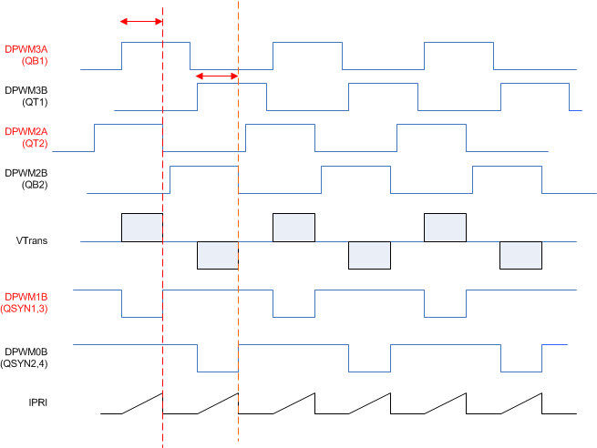 Figure 6-6 Phase Shifted Full Bridge
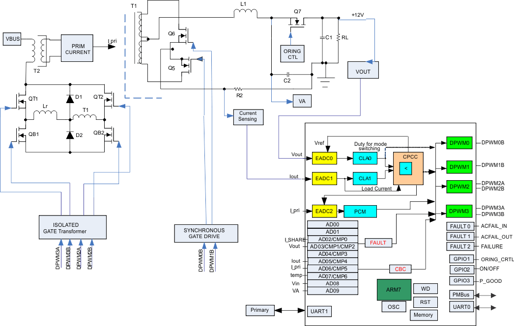 Figure 6-7 Secondary-Referenced Phase-Shifted Full Bridge Control
 With Synchronous Rectification
6.7.2 LLC Example
In LLC, three modes are used. At the highest frequency, a pulse width modulated mode (Multi Mode) is used. As the frequency decreases, resonant mode is used. As the frequency gets still lower, the synchronous MOSFET drive changes so that the on-time is fixed and does not increase. In addition, the LLC control supports cycle-by-cycle current limiting. This protection function operates by a comparator monitoring the maximum current during the DPWMA conduction time. Any time this current exceeds the programmable comparator reference the pulse is immediately terminated. Due to classic instability issues associated with half-bridge topologies it is also possible to force DPWMB to match the truncated pulse width of DPWMA. Here are the waveforms for the LLC:

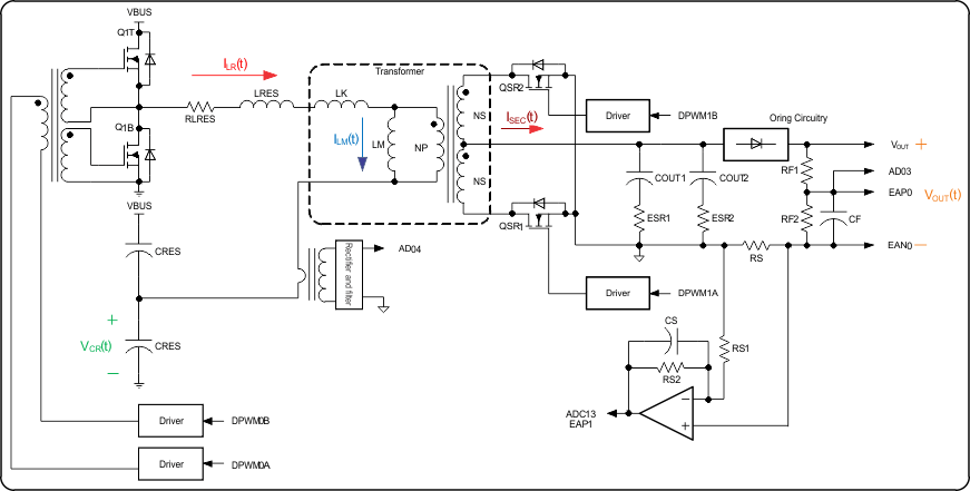 Figure 6-8 Secondary-Referenced Half-Bridge Resonant LLC Control
 With Synchronous Rectification
6.7.3 Mechanism for Automatic Mode Switching
The UCD3138A allows the customer to enable up to two distinct levels of automatic mode switching. These different modes are used to enhance light load operation, short circuit operation and soft start. Many of the configuration parameters for the DPWM are in DPWM Control Register 1. For automatic mode switching, some of these parameters are duplicated in the Auto Config Mid and Auto Config High registers.
If automatic mode switching is enabled, the filter duty signal is used to select which of these three registers is used. There are 4 registers which are used to select the points at which the mode switching takes place. They are used as shown in Figure 6-9.
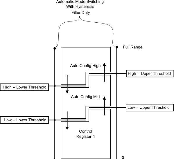 Figure 6-9 Automatic Mode Switching
As shown, the registers are used in pairs for hysteresis. The transition from Control Register 1 to Auto Config Mid only takes place when the Filter Duty goes above the Low Upper threshold. It does not go back to Auto Config Mid until the Low Lower Threshold is passed. This prevents oscillation between modes if the filter duty is close to a mode switching point.
6.8 DPWMC, Edge Generation, IntraMux
The UCD3138A has hardware for generating complex waveforms beyond the simple DPWMA and DPWMB waveforms already discussed – DPWMC, the Edge Generation Module, and the IntraMux.
DPWMC is an auxillary signal inside the DPWM logic. It can be generated using the Blanking A begin time, and the Blanking A end time.
The Edge Gen module takes DPWMA and DPWMB from its own DPWM module, and the next one, and uses them to generate edges for two outputs. For DPWM3, the DPWM0 is considered to be the next DPWM. Each edge (rising and falling for DPWMA and DPWMB) has 8 options which can output a generated edge.
The options are:
0 = DPWM(n) A Rising edge
1 = DPWM(n) A Falling edge
2 = DPWM(n) B Rising edge
3 = DPWM(n) B Falling edge
4 = DPWM(n+1) A Rising edge
5 = DPWM(n+1) A Falling edge
6 = DPWM(n+1) B Rising edge
7 = DPWM(n+1) B Falling edge
Where “n" is the numerical index of the DPWM module of interest. For example n=1 refers to DPWM1.
The Edge Gen is controlled by the DPWMEDGEGEN register.
The IntraMux (short for intra multiplexer) is controlled by the Auto Config registers. The IntraMux takes signals from multiple DPWMs and from the Edge Gen and combines them logically to generate DPWMA and DPWMB signals This is useful for topologies like phase-shifted full bridge, especially when they are controlled with automatic mode switching. Of course, it can all be disabled, and DPWMA and DPWMB will be driven as described in the sections above. If the Intra Mux is enabled, high resolution must be disabled, and DPWM edge resolution goes down to 4 ns.
The Edge Gen/Intra Mux is shown in Figure 6-10.
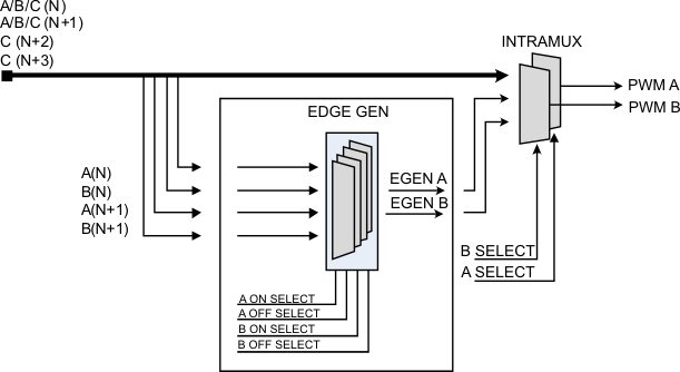 Figure 6-10 Edge Gen/Intra Mux
A list of the IntraMux modes for DPWMA is as follows:
0 = DPWMA(n) pass through (default)
1 = Edge-gen output, DPWMA(n)
2 = DPWNC(n)
3 = DPWMB(n) (Crossover)
4 = DPWMA(n+1)
5 = DPWMB(n+1)
6 = DPWMC(n+1)
7 = DPWMC(n+2)
8 = DPWMC(n+3)
0 = DPWMB(n) pass through (default)
1 = Edge-gen output, DPWMB(n)
2 = DPWNC(n)
3 = DPWMA(n) (Crossover)
4 = DPWMA(n+1)
5 = DPWMB(n+1)
6 = DPWMC(n+1)
7 = DPWMC(n+2)
8 = DPWMC(n+3)
The DPWM number wraps around just like the Edge Gen unit. For DPWM3 the following definitions apply:
| DPWM(n) | DPWM3 |
| DPWM(n+1) | DPWM0 |
| DPWM(n+2) | DPWM1 |
| DPWM(n+3) | DPWM2 |
6.9 Filter
The UCD3138A filter is a PID filter with many enhancements for power supply control. Some of its features include:
- Traditional PID Architecture
- Programmable non-linear limits for automated modification of filter coefficients based on received EADC error
- Multiple coefficient sets fully configurable by firmware
- Full 24-bit precision throughout filter calculations
- Programmable clamps on integrator branch and filter output
- Ability to load values into internal filter registers while system is running
- Ability to stall calculations on any of the individual filter branches
- Ability to turn off calculations on any of the individual filter branches
- Duty cycle, resonant period, or phase shift generation based on filter output.
- Flux balancing
- Voltage feed forward
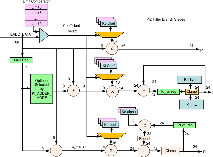 Figure 6-11 First Section of the Filter
The filter input, Xn, generally comes from a front end. Then there are three branches, P, I. and D. Note that the D branch also has a pole, Kd Alpha. Clamps are provided both on the I branch and on the D alpha pole.
The filter also supports a nonlinear mode, where up to 7 different sets of coefficients can be selected depending on the magnitude of the error input Xn. This can be used to increase the filter gain for higher errors to improve transient response.
Tthe output section of the filter (S0.23 means that there is 1 sign bit, 0 integer bits and 23 fractional bits) is shown in Figure 6-12
 Figure 6-12 Output Section of the Filter
This section combines the P, I, and D sections, and provides for saturation, scaling, and clamping.
The final section for the filter, which permits its output to be matched to the DPWM is shown in Figure 6-13.
 Figure 6-13 Final Section for the Filter
This permits the filter output to be multiplied by a variety of correction factors to match the DPWM Period, to provide for Voltage Feed Forward, or for other purposes. After this, there is another clamp. For resonant mode, the filter can be used to generate both period and duty cycle.
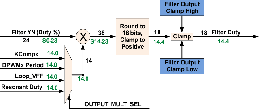 Figure 6-14 Resonant Mode
6.9.1 Loop Multiplexer
The Loop Mux controls interconnections between the filters, front ends, and DPWMs. Any filter, front end, and DPWM can be combined with each other in many configurations.
It also controls the following connections:
- DPWM to Front End
- Front End DAC control from Filters or Constant Current/Constant Power Module
- Filter Special Coefficients and Feed Forward
- DPWM synchronization
- Filter to DPWM
The following control modules are configured in the Loop Mux:
- Constant Power/Constant Current
- Cycle Adjustment (Current and flux balancing)
- Global Period
- Light Load (Burst Mode)
- Analog Peak Current Mode
6.9.2 Fault Multiplexer
In order to allow a flexible way of mapping several fault triggering sources to all the DPWMs channels, the UCD3138A provides an extensive array of multiplexers that are united under the name Fault Mux module.
The Fault Mux Module supports flexible mapping between fault sources and fault response mechanism inside each DPWM module.
- Many fault sources can be mapped to a single fault response mechanism. For instance an analog comparator in charge of over voltage protection, a digital comparator in charge of over current protection and an external digital fault pin can be all mapped to a fault-A signal connected to a single FAULT MODULE and shut down DPWM1-A.
- A single fault source can be mapped to many fault response mechanisms inside many DPWM modules. For instance an analog comparator in charge of over current protection can be mapped to DPWM-0 through DPWM-3 by way of several fault modules.
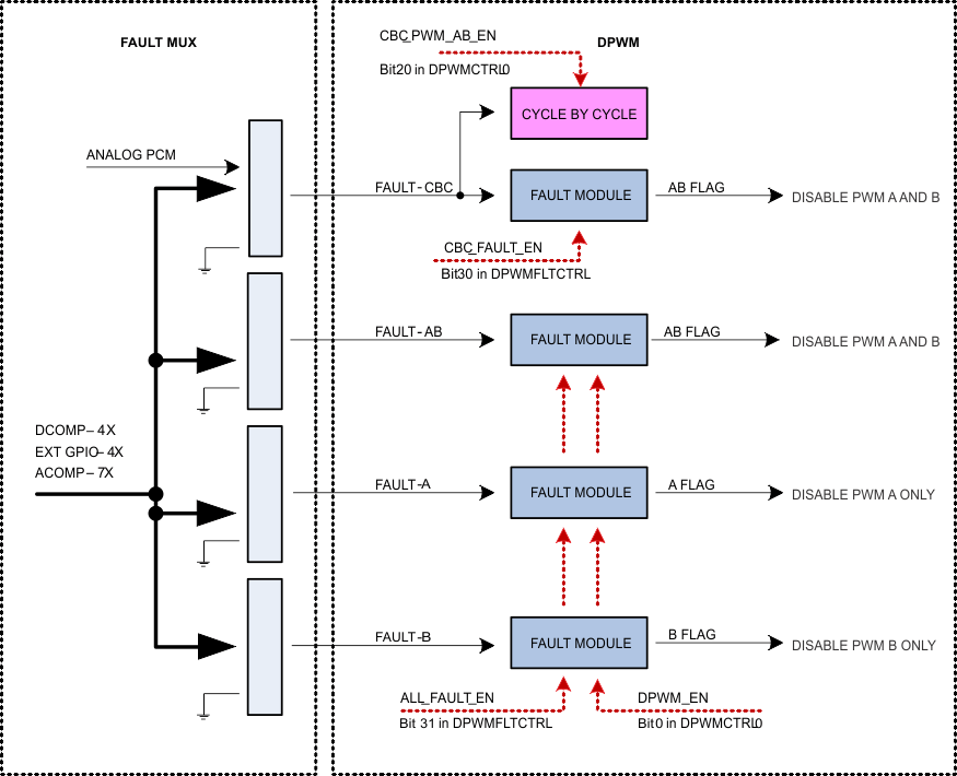
The Fault Mux Module provides a multitude of fault protection functions within the UCD3138A high-speed loop (front end control, filter, DPWM and loop Mux modules). The Fault Mux Module allows highly configurable fault generation based on digital comparators, high-speed analog comparators and external fault pins. Each of the fault inputs to the DPWM modules can be configured to one or any combination of the fault events provided in the Fault Mux Module.
Each one of the DPWM engines has four fault modules. The modules are called CBC fault module, AB fault module, A fault module and B fault module.
The internal circuitry in all the four fault modules is identical, and the difference between the modules is limited to the output it affects under a fault condition.
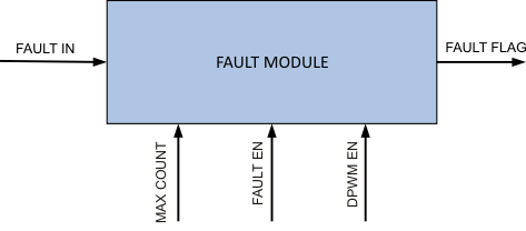 Figure 6-15 Fault Module
All fault modules are capable of detecting faults only once per DPWM switching cycle. Each one of the fault modules have a separate max_count and the fault flag will be set only if sequential faults count exceeds max_count.
Once the fault flag is set DPWMs need to be disabled by DPWM_EN going low in order to clear the fault flags. Note, all four Fault Modules share the same DPWM_EN control, all fault flags (output of Fault Modules) is cleared simultaneously.
All four Fault Modules share the same global FAULT_EN as well. Therefore, a specific Fault Module cannot be enabled/ disabled separately.
 Figure 6-16 Cycle by Cycle Block
In contrast to the fault modules, only one cycle by cycle block is available in each DPWM module.
The cycle by cycle block can work in conjunction with CBC Fault Module and enables DPWM reaction to signals arriving from analog peak current mode (PCM) module.
The fault Mux module supports the following basic functions:
- 4 digital comparators with programmable thresholds and fault generation
- Configuration for 7 high-speed analog comparators with programmable thresholds and fault generation
- External GPIO detection control with programmable fault generation
- Configurable DPWM fault generation for DPWM current limit fault, DPWM overvoltage detection fault, DPWM A external fault, DPWM B external fault and DPWM IDE flag
- Clock failure detection for high and low frequency oscillator blocks
- Discontinuous conduction mode detection
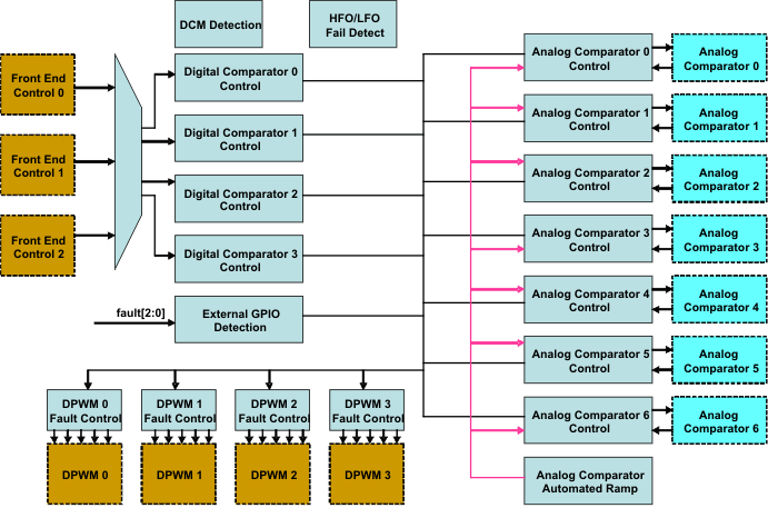 Figure 6-17 Fault Mux Block Diagram
6.10 Communication Ports
6.10.1 SCI (UART) Serial Communication Interface
A maximum of two independent Serial Communication Interface (SCI) or Universal Asynchronous Receiver/Transmitter pre-scaler (UART) interfaces are included within the device for asynchronous start-stop serial data communication (see the pin out sections for details) Each interface has a 24 bit for supporting programmable baud rates and has programmable data word and stop bit options. Half or full duplex operation is configurable through register bits. A loop back feature can also be setup for firmware verification. Both SCI-TX and SCI-RX pin sets can be used as GPIO pins when the peripheral is not being used. Both the UART ports support Hardware auto baud correction improving robustness in communication even at higher baud rates.
6.10.2 PMBUS
The PMBus Interface supports independent master and slave modes controlled directly by firmware through a processor bus interface. Individual control and status registers enable firmware to send or receive I2C, SMBus or PMBus messages in any of the accepted protocols, in accordance with the I2C Specification, SMBus Specification (Version 2.0) and the PMBUS Power System Management Protocol Specification (PMBus 1.3).
The PMBus interface is controlled through a processor bus interface, utilizing a 32-bit data bus and 6-bit address bus. The PMBus interface is connected to the expansion bus, which features 4 byte write enables, a peripheral select dedicated for the PMBus interface, separated 32-bit data buses for reading and writing of data and active-low write and output enable control signals. In addition, the PMBus Interface connects directly to the I2C/SMBus/PMBus Clock, Data, Alert, and Control signals.
Example: PMBus Address Decode via ADC12 Reading
The user can allocate 2 pins of the 12-bit ADC input channels, AD_00 and AD_01, for PMBus address decoding. At power-up the device applies IBIAS to each address detect pin and the voltage on that pin is captured by the internal 12-bit ADC.
Where bin(VAD0x) is the address bin for one of 12 address as shown in Figure 6-18.
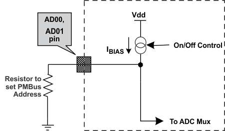 Figure 6-18 PMBus Address Detection Method
6.10.3 General Purpose ADC12
The ADC12 is a 12 bit, high speed analog to digital converter, equipped with the following options:
- Typical conversion speed of 267 ksps
- Conversions can consist from 1 to 16 ADC channel conversions in any desired sequence
- Post conversion averaging capability, ranging from 4X, 8X, 16X or 32X samples
- Configurable triggering for ADC conversions from the following sources: firmware, DPWM rising edge, ADC_EXT_TRIG pin or Analog Comparator results
- Interrupt capability to embedded processor at completion of ADC conversion
- Six digital comparators on the first 6 channels of the conversion sequence using either raw ADC data or averaged ADC data
- Two 10 µA current sources for excitation of PMBus addressing resistors
- Dual sample and hold for accurate power measurement
- Internal temperature sensor for temperature protection and monitoring
The control module ADC12 Contol Block Diagram contains the control and conversion logic for auto-sequencing a series of conversions. The sequencing is fully configurable for any combination of 16 possible ADC channels through an analog multiplexer embedded in the ADC12 block. Once converted, the selected channel value is stored in the result register associated with the sequence number. Input channels can be sampled in any desired order or programmed to repeat conversions on the same channel multiple times during a conversion sequence. Selected channel conversions are also stored in the result registers in order of conversion, where the result 0 register is the first conversion of a 16-channel sequence and result 15 register is the last conversion of a 16-channel sequence. The number of channels converted in a sequence can vary from 1 to 16.
Unlike EADC0 through EADC2, which are primarily designed for closing high speed compensation loops, the ADC12 is not usually used for loop compensation purposes. The EADC converters have a substantially faster conversion rate, thus making them more attractive for closed loop control. The ADC12 features make it best suited for monitoring and detection of currents, voltages, temperatures and faults. Please see the Typical Characteristics plots for the temperature variation associated with this function.
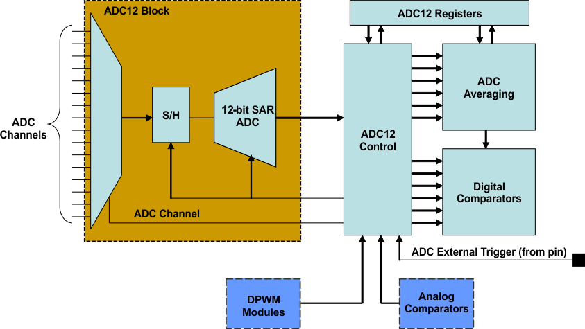 Figure 6-19 ADC12 Control Block Diagram
6.10.4 Timers
External to the Digital Power Peripherals there are 3 different types of timers in UCD3138A. They are the 24-bit timer, 16-bit timer and the Watchdog timer
6.10.4.1 24-bit PWM Timer
There is one 24 bit counter PWM timer which runs off the Interface Clock and can further be divided down by an 8-bit pre-scalar to generate a slower PWM time period. The timer has two compare registers (Data Registers) for generating the PWM set/unset events. Additionally, the timer has a shadow register (Data Buffer register) which can be used to store CPU updates of the compare events while still using the timer. The selected shadow register update mode happens after the compare event matches.
The two capture pins TCMP0 and TCMP1 are inputs for recording a capture event. A capture event can be set either to rising, falling, or both edges of the capture pin. Upon this event, the counter value is stored in the corresponding capture data register.
The counter reset can be configured to happen on a counter roll over, a compare equal event, or by software controlled register. Five Interrupts from the PWM timer can be set, which are the counter rollover event (overflow), either capture event 0 or 1, or the two comparison match events. Each interrupt can be disabled or enabled.
Upon an event comparison on only the second event, the TCMP pin can be configured to set, clear, toggle or have no action at the output. The value of PWM pin output can be read for status or simply configured as general purpose I/O for reading the value of the input at the pin. The first compare event can only be used as an interrupt.
6.10.4.2 16-Bit PWM Timers
There are four 16 bit counter PWM timers which run off the Interface Clock and can further be divided down by a 8-bit pre-scaler to generate slower PWM time periods. Each timer has two compare registers (Data Registers) for generating the PWM set/unset events. Additionally, each timer has a shadow register (Data Buffer register) which can be used to store CPU updates of compare events while still using the timer. The selected shadow register update mode happens after the compare event matches.
The counter reset can be configured to happen on a counter roll over, a compare equal event, or by a software controlled register. Interrupts from the PWM timer can be set due to the counter rollover event (overflow) or by the two comparison match events. Each comparison match and the overflow interrupts can be disabled or enabled.
Upon an event comparison, the PWM pin can be configured to set, clear, toggle or have no action at the output. The value of PWM pin output can be read for status or simply configured as General Purpose I/O for reading the value of the input at the pin.
6.10.4.3 Watchdog Timer
A watchdog timer is provided on the device for ensuring proper firmware loop execution. The timer is clocked off of a separate low speed oscillator source. If the timer is allowed to expire, a reset condition is issued to the ARM processor. The watchdog is reset by a simple CPU write bit to the watchdog key register by the firmware routine. On device power-up the watchdog is disabled. Yet after it is enabled, the watchdog cannot be disabled by firmware. Only a device reset can put this bit back to the default disabled state. A half timer flag is also provided for status monitoring of the watchdog.
6.11 Miscellaneous Analog
The Miscellaneous Analog Control (MAC) Registers provide control and monitor a wide variety of functions. These functions include device supervisory features such as Brown-Out and power saving configuration, general purpose input/output configuration and interfacing, internal temperature sensor control and current sharing control.
The MAC module also provides trim signals to the oscillator and AFE blocks. These controls are usually used at the time of trimming at manufacturing; therefore this document will not cover these trim controls.
The MAC registers and peripherals are all available in the UCD3138A (64 pin version). Other UCD3138A devices may have reduced resources. See the device pin out description for details.
6.12 Package ID Information
Package ID register includes information regarding the package type of the device and can be read by firmware for reporting through PMBus or for other package sensitive decisions.
| BIT NUMBER | 1:0 |
|---|---|
| Bit Name | PKG_ID |
| Access | R/W |
| Default | 0 – UCD3138ARGC, 1 – UCD3138ARHA |
6.13 Brownout
Brownout function is used to determine if the device supply voltage is lower than a threshold voltage, a condition that may be considered unsafe for proper operation of the device.
The brownout threshold is higher than the reset threshold voltage; therefore, when the supply voltage is lower than brownout threshold, it still does not necessarily trigger a device reset.
The brownout interrupt flag can be polled or alternatively can trigger an interrupt to service such case by an interrupt service routine. See Section 5.7.
6.14 Global I/O
Up to 30 pins in UCD3138A can be configured to serve as a general purpose input or output pin (GPIO). This includes all digital input or output pins except for the RESET pin.
The pins that cannot be configured as GPIO pins are the supply pins, ground pins, ADC-12 analog input pins, EADC analog input pins and the RESET pin.
There are two ways to configure and use the digital pins as GPIO pins:
- Through the centralized Global I/O control registers.
- Through the distributed control registers in the specific peripheral that shares it pins with the standard GPIO functionality.
The Global I/O registers offer full control of:
- Configuring each pin as a GPIO.
- Setting each pin as input or output.
- Reading the pin’s logic state, if it is configured as an input pin.
- Setting the logic state of the pin, if it is configured as an output pin.
- Configuring pin/pins as open drain or push-pull (Normal)
The Global I/O registers include Global I/O EN register, Global I/O OE Register, Global I/O Open Drain Control Register, Global I/O Value Register and Global I/O Read Register.
The following is showing the format of Global I/O EN Register (GLBIOEN) as an example:
| BIT NUMBER | 29:0 |
|---|---|
| Bit Name | GLOBAL_IO_EN |
| Access | R/W |
| Default | 00_0000_0000_0000_0000_0000_0000_0000 |
Bits 29-0: GLOBAL_IO_EN – This register enables the global control of digital I/O pins
0 = Control of IO is done by the functional block assigned to the IO (Default)
1 = Control of IO is done by Global IO registers.
| BIT | PIN_NAME | PIN NUMBER | |
|---|---|---|---|
| UCD3138A-64 PINS | UCD3138A-40 PINS | ||
| 29 | FAULT[3] | 43 | NA |
| 28 | ADC_EXT_TRIG | 12, 26 | 8 |
| 27 | TCK | 37 | 21 |
| 26 | TDO | 38 | 20 |
| 25 | TMS | 40 | 24 |
| 24 | TDI | 39 | 23 |
| 23 | SCI_TX[1] | 29 | NA |
| 22 | SCI_TX[0] | 14 | 22 |
| 21 | SCI_RX[1] | 30 | NA |
| 20 | SCI_RX[0] | 13 | 23 |
| 19 | TMR_CAP | 12, 26, 41 | 8, 21 |
| 18 | TMR_PWM[1] | 32 | NA |
| 17 | TMR_PWM[0] | 12, 26, 31, 37 | 21 |
| 16 | PMBUS-CLK | 15 | 9 |
| 15 | PMBUS-DATA | 16 | 10 |
| 14 | CONTROL | 30 | 20 |
| 13 | ALERT | 29 | 19 |
| 12 | EXT_INT | 26, 34 | NA |
| 11 | FAULT[2] | 42 | 25 |
| 10 | FAULT[1] | 36 | 23 |
| 9 | FAULT[0] | 35, 39 | 22 |
| 8 | SYNC | 12, 26,37 | 8, 21 |
| 7 | DPWM3B | 24 | 18 |
| 6 | DPWM3A | 23 | 17 |
| 5 | DPWM2B | 22 | 16 |
| 4 | DPWM2A | 21 | 15 |
| 3 | DPWM1B | 20 | 14 |
| 2 | DPWM1A | 19 | 13 |
| 1 | DPWM0B | 18 | 12 |
| 0 | DPWM0A | 17 | 11 |
6.15 Temperature Sensor Control
Temperature sensor control register provides internal temperature sensor enabling and trimming capabilities. The internal temperature sensor is disabled as default.
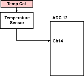 Figure 6-20 Internal Temp Sensor
Temperature sensor is calibrated at room temperature (25°C) via a calibration register value.
The temperature sensor is measured using ADC12 (via Ch14). The temperature is then calculated using a mathematical formula involving the calibration register (this effectively adds a delta to the ADC measurement).
The temperature sensor can be enabled or disabled.
6.16 I/O Mux Control
In different packages of UCD3138A several I/O functions are multiplexed and routed toward a single physical pin. I/O Mux Control register may be used in order to choose a single specific functionality that is desired to be assigned to a physical device pin for your application.
6.17 Current Sharing Control
UCD3138A provides three separate modes of current sharing operation.
- Analog bus current sharing
- PWM bus current sharing
- Master/Slave current sharing
- AD02 has a special ESD protection mechanism that prevents the pin from pulling down the current-share bus if power is missing from the UCD3138A
The simplified current sharing circuitry is shown in the drawing below:
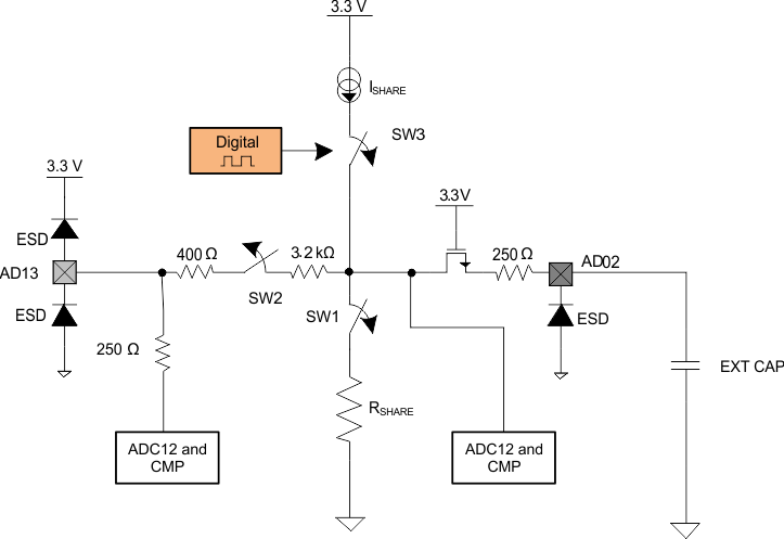 Figure 6-21 Simplified Current Sharing Circuitry
| CURRENT SHARING MODE | FOR TEST ONLY, ALWAYS KEEP 00 |
CS_MODE | EN_SW1 | EN_SW2 | DPWM |
|---|---|---|---|---|---|
| Off or Slave Mode (3-state) | 00 | 00 (default) | 0 | 0 | 0 |
| PWM Bus | 00 | 01 | 1 | 0 | ACTIVE |
| Off or Slave Mode (3-state) | 00 | 10 | 0 | 0 | 0 |
| Analog Bus or Master | 00 | 11 | 0 | 1 | 0 |
The period and the duty of 8-bit PWM current source and the state of the SW1 and SW2 switches can be controlled through the current sharing control register (CSCTRL).
6.18 Temperature Reference
The temperature reference register (TEMPREF) provides the ADC12 count when ADC12 measures the internal temperature sensor (channel 14) during the factory trim and calibration.
This information can be used by different periodic temperature compensation routines implemented in the firmware. But it should not be overwritten by firmware, otherwise this factory written value will be lost.