ZHCSDJ8A March 2015 – April 2015 UCD3138A
PRODUCTION DATA.
- 1器件概述
- 2修订历史记录
- 3Device Comparison
- 4Terminal Configuration and Functions
- 5Specifications
-
6Detailed Description
- 6.1 Overview
- 6.2 ARM Processor
- 6.3 Memory
- 6.4 System Module
- 6.5 DPWM Modes of Operation
- 6.6 Sync FET Ramp and IDE Calculation
- 6.7 Automatic Mode Switching
- 6.8 DPWMC, Edge Generation, IntraMux
- 6.9 Filter
- 6.10 Communication Ports
- 6.11 Miscellaneous Analog
- 6.12 Package ID Information
- 6.13 Brownout
- 6.14 Global I/O
- 6.15 Temperature Sensor Control
- 6.16 I/O Mux Control
- 6.17 Current Sharing Control
- 6.18 Temperature Reference
-
7Application, Implementation, and Layout
- 7.1 Application Information
- 7.2 Typical Application
- 7.3 Layout
- 7.4 Power Supply Decoupling and Bulk Capacitors
- 8器件和文档支持
- 9机械封装和可订购信息
封装选项
机械数据 (封装 | 引脚)
散热焊盘机械数据 (封装 | 引脚)
订购信息
4 Terminal Configuration and Functions
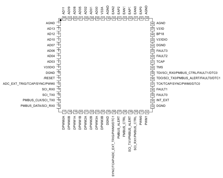
4.1 UCD3138ARGC Package
64 QFN PACKAGE
TOP VIEW

Table 4-1 UCD3138ARGC Terminal Functions
| PIN NO. | NAME | PRIMARY ASSIGNMENT | ALTERNATE ASSIGNMENT | CONFIGURABLE AS A GPIO? |
|||
|---|---|---|---|---|---|---|---|
| NO. 1 | NO. 2 | NO. 3 | NO. 4 | ||||
| 1 | AGND | Analog ground | |||||
| 2 | AD13 | 12-bit ADC, Ch 13, comparator E, I-share | DAC output | ||||
| 3 | AD12 | 12-bit ADC, Ch 12 | |||||
| 4 | AD10 | 12-bit ADC, Ch 10 | |||||
| 5 | AD07 | 12-bit ADC, Ch 7, Connected to comparator F and reference to comparator G | DAC output | ||||
| 6 | AD06 | 12-bit ADC, Ch 6, Connected to comparator F | DAC output | ||||
| 7 | AD04 | 12-bit ADC, Ch 4, Connected to comparator D | DAC output | ||||
| 8 | AD03 | 12-bit ADC, Ch 3, Connected to comparator B and C | |||||
| 9 | V33DIO | Digital I/O 3.3V core supply | |||||
| 10 | DGND | Digital ground | |||||
| 11 | RESET | Device Reset Input, active low | |||||
| 12 | ADC_EXT_TRIG | ADC conversion external trigger input | TCAP | SYNC | PWM0 | Yes | |
| 13 | SCI_RX0 | SCI RX 0 | Yes | ||||
| 14 | SCI_TX0 | SCI TX 0 | Yes | ||||
| 15 | PMBUS_CLK | PMBUS Clock (Open Drain) | SCI TX 0 | Yes | |||
| 16 | PMBUS_DATA | PMBus data (Open Drain) | SCI RX 0 | Yes | |||
| 17 | DPWM0A | DPWM 0A output | Yes | ||||
| 18 | DPWM0B | DPWM 0B output | Yes | ||||
| 19 | DPWM1A | DPWM 1A output | Yes | ||||
| 20 | DPWM1B | DPWM 1B output | Yes | ||||
| 21 | DPWM2A | DPWM 2A output | Yes | ||||
| 22 | DPWM2B | DPWM 2B output | Yes | ||||
| 23 | DPWM3A | DPWM 3A output | Yes | ||||
| 24 | DPWM3B | DPWM 3B output | Yes | ||||
| 25 | DGND | Digital ground | |||||
| 26 | SYNC | DPWM Synchronize pin | TCAP | ADC_EXT_TRIG | PWM0 | DTC1 | Yes |
| 27 | PMBUS_ALERT | PMBus Alert (Open Drain) | Yes | ||||
| 28 | PMBUS_CTRL | PMBus Control (Open Drain) | Yes | ||||
| 29 | SCI_TX1 | SCI TX 1 | PMBUS_ALERT | Yes | |||
| 30 | SCI_RX1 | SCI RX 1 | PMBUS_CTRL | Yes | |||
| 31 | PWM0 | General purpose PWM 0 | Yes | ||||
| 32 | PWM1 | General purpose PWM 1 | Yes | ||||
| 33 | DGND | Digital ground | |||||
| 34 | INT_EXT | External Interrupt | Yes | ||||
| 35 | FAULT0 | External fault input 0 | Yes | ||||
| 36 | FAULT1 | External fault input 1 | Yes | ||||
| 37 | TCK | JTAG TCK | TCAP | SYNC | PWM0 | DTC0 | Yes |
| 38 | TDO | JTAG TDO | SCI_TX0 | PMBUS_ALERT | FAULT0 | DTC1 | Yes |
| 39 | TDI | JTAG TDI | SCI_RX0 | PMBUS_CTRL | FAULT1 | DTC0 | Yes |
| 40 | TMS | JTAG TMS | Yes | ||||
| 41 | TCAP | Timer capture input | Yes | ||||
| 42 | FAULT2 | External fault input 2 | Yes | ||||
| 43 | FAULT3 | External fault input 3 | Yes | ||||
| 44 | DGND | Digital ground | |||||
| 45 | V33DIO | Digital I/O 3.3V core supply | |||||
| 46 | BP18 | 1.8V Bypass | |||||
| 47 | V33D | Digital 3.3V core supply | |||||
| 48 | AGND | Substrate analog ground | |||||
| 49 | AGND | Analog ground | |||||
| 50 | EAP0 | Channel 0, differential analog voltage, positive input | |||||
| 51 | EAN0 | Channel 0, differential analog voltage, negative input | |||||
| 52 | EAP1 | Channel 1, differential analog voltage, positive input | |||||
| 53 | EAN1 | Channel 1, differential analog voltage, negative input | |||||
| 54 | EAP2 | Channel 2, differential analog voltage, positive input (Recommended for peak currrent mode control) |
|||||
| 55 | EAN2 | Channel #2, differential analog voltage, negative input | |||||
| 56 | AGND | Analog ground | |||||
| 57 | V33A | Analog 3.3-V supply | |||||
| 58 | AD00 | 12-bit ADC, Ch 0, Connected to current source | |||||
| 59 | AD01 | 12-bit ADC, Ch 1, Connected to current source | |||||
| 60 | AD02 | 12-bit ADC, Ch 2, Connected to comparator A, I-share | |||||
| 61 | AD05 | 12-bit ADC, Ch 5 | |||||
| 62 | AD08 | 12-bit ADC, Ch 8 | |||||
| 63 | AD09 | 12-bit ADC, Ch 9 | |||||
| 64 | AD11 | 12-bit ADC, Ch 11 | |||||
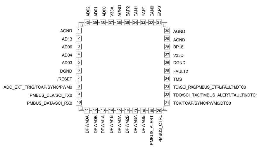
4.2 UCD3138ARMH Package
40 QFN PACKAGE
With Corner Anchors Pin Attributes
TOP VIEW

NOTE: The RMH package has thinner package height compared to the RHA package. There are also four corner pins on the RMH package. These features help to improve solder-joint reliability. The corner anchor pins and thermal pad should be soldered for robust mechanical performance and should be tied to the appropriate ground signal.
Table 4-2 UCD3138ARMH Terminal Functions
| PIN NO. | NAME | PRIMARY ASSIGNMENT | ALTERNATE ASSIGNMENT | CONFIGURABLE AS A GPIO? |
|||
|---|---|---|---|---|---|---|---|
| NO. 1 | NO. 2 | NO. 3 | NO. 4 | ||||
| 1 | AGND | Analog ground | |||||
| 2 | AD13 | 12-bit ADC, Ch 13, Connected to comparator E, I-share | |||||
| 3 | AD06 | 12-bit ADC, Ch 6, Connected to comparator F | |||||
| 4 | AD04 | 12-bit ADC, Ch 4, Connected to comparator D | |||||
| 5 | AD03 | 12-bit ADC, Ch 3, Connected to comparator B and C | |||||
| 6 | DGND | Digital ground | |||||
| 7 | RESET | Device Reset Input, active low | |||||
| 8 | ADC_EXT_TRIG | ADC conversion external trigger input | TCAP | SYNC | PWM0 | Yes | |
| 9 | PMBUS_CLK | PMBUS Clock (Open Drain) | SCI_TX0 | Yes | |||
| 10 | PMBUS_DATA | PMBus data (Open Drain) | SCI_RX0 | Yes | |||
| 11 | DPWM0A | DPWM 0A output | Yes | ||||
| 12 | DPWM0B | DPWM 0B output | Yes | ||||
| 13 | DPWM1A | DPWM 1A output | Yes | ||||
| 14 | DPWM1B | DPWM 1B output | Yes | ||||
| 15 | DPWM2A | DPWM 2A output | Yes | ||||
| 16 | DPWM2B | DPWM 2B output | Yes | ||||
| 17 | DWPM3A | DPWM 3A output | Yes | ||||
| 18 | DPWM3B | DPWM 3B output | Yes | ||||
| 19 | PMBUS_ALERT | PMBus Alert (Open Drain) | Yes | ||||
| 20 | PMBUS_CTRL | PMBus Control (Open Drain) | Yes | ||||
| 21 | TCK | JTAG TCK | TCAP | SYNC | PWM0 | DTC0 | Yes |
| 22 | TDO | JTAG TDO | SCI_TX0 | PMBUS_ALERT | FAULT0 | DTC1 | Yes |
| 23 | TDI | JTAG TDI | SCI_RX0 | PMBUS_CTRL | FAULT1 | DTC0 | Yes |
| 24 | TMS | JTAG TMS | Yes | ||||
| 25 | FAULT2 | External fault input 2 | Yes | ||||
| 26 | DGND | Digital ground | |||||
| 27 | V33D | Digital 3.3V core supply | |||||
| 28 | BP18 | 1.8V Bypass | |||||
| 29 | AGND | Substrate analog ground | |||||
| 30 | AGND | Analog ground | |||||
| 31 | EAP0 | Channel 0, differential analog voltage, positive input | |||||
| 32 | EAN0 | Channel 0, differential analog voltage, negative input | |||||
| 33 | EAP1 | Channel 1, differential analog voltage, positive input | |||||
| 34 | EAN1 | Channel 1, differential analog voltage, negative input | |||||
| 35 | EAP2 | Channel 2, differential analog voltage, positive input (Recommended for peak currrent mode control) |
|||||
| 36 | AGND | Analog ground | |||||
| 37 | V33A | Analog 3.3-V supply | |||||
| 38 | AD00 | 12-bit ADC, Ch 0, Connected to current source | |||||
| 39 | AD01 | 12-bit ADC, Ch 1, Connected to current source | |||||
| 40 | AD02 | 12-bit ADC, Ch 2, Connected to comparator A, I-share | |||||
| Corner NA |
Corner anchor pin |
All four anchors should be soldered and tied to GND | |||||