SLUSC99A July   2016  – January 2017 UCD3138128A

PRODUCTION DATA.  

  1. Features
  2. Applications
  3. Description
  4. Revision History
  5. Device Comparison
  6. Pin Configuration and Functions
  7. Specifications
    1. 7.1 Absolute Maximum Ratings
    2. 7.2 ESD Ratings
    3. 7.3 Recommended Operating Conditions
    4. 7.4 Thermal Information
    5. 7.5 Electrical Characteristics
    6. 7.6 Timing Characteristics
    7. 7.7 PMBus/SMBus/I2C Timing
    8. 7.8 Typical Characteristics
    9. 7.9 Timing Diagrams
  8. Parametric Measurement Information
    1. 8.1 Typical Clock Gating Power Savings
  9. Detailed Description
    1. 9.1 Overview
      1. 9.1.1 ARM Processor
      2. 9.1.2 Memory
    2. 9.2 Functional Block Diagram
    3. 9.3 Feature Description
      1. 9.3.1  System Module
        1. 9.3.1.1 Address Decoder (DEC)
        2. 9.3.1.2 Memory Management Controller (MMC)
        3. 9.3.1.3 System Management (SYS)
        4. 9.3.1.4 Central Interrupt Module (CIM)
      2. 9.3.2  Peripherals
        1. 9.3.2.1 Digital Power Peripherals (DPPs)
          1. 9.3.2.1.1 Front End
          2. 9.3.2.1.2 DPWM Module
          3. 9.3.2.1.3 DPWM Events
          4. 9.3.2.1.4 High Resolution DPWM
          5. 9.3.2.1.5 Oversampling
          6. 9.3.2.1.6 DPWM Interrupt Generation
          7. 9.3.2.1.7 DPWM Interrupt Scaling/Range
          8. 9.3.2.1.8 Synchronous Rectifier Dead Time Optimization Peripheral
      3. 9.3.3  Automatic Mode Switching
        1. 9.3.3.1 Phase Shifted Full Bridge Example
        2. 9.3.3.2 LLC Example
        3. 9.3.3.3 Mechanism For Automatic Mode Switching
      4. 9.3.4  DPWMC, Edge Generation, Intramux
      5. 9.3.5  Synchronous Rectifier MOSFET Ramp And IDE Calculation
      6. 9.3.6  Filter
        1. 9.3.6.1 Loop Multiplexer
        2. 9.3.6.2 Fault Multiplexer
      7. 9.3.7  Communication Ports
        1. 9.3.7.1 SCI (UART) Serial Communication Interface
        2. 9.3.7.2 PMBUS/I2C
          1. 9.3.7.2.1 Example: PMBus Address Decode via ADC12 Reading
        3. 9.3.7.3 SPI
        4. 9.3.7.4 JTAG Standard Interface
      8. 9.3.8  Real Time Clock
      9. 9.3.9  External Crystal Interface
      10. 9.3.10 Timers
        1. 9.3.10.1 24-Bit Timer
        2. 9.3.10.2 16-Bit PWM Timers
        3. 9.3.10.3 Watchdog Timer
      11. 9.3.11 General Purpose ADC12
      12. 9.3.12 Miscellaneous Analog
      13. 9.3.13 Brownout
      14. 9.3.14 Global I/O
      15. 9.3.15 Temperature Sensor Control
      16. 9.3.16 I/O Mux Control
      17. 9.3.17 Current Sharing Control
      18. 9.3.18 Temperature Reference
    4. 9.4 Device Functional Modes
      1. 9.4.1 DPWM Modes of Operation
        1. 9.4.1.1 Normal Mode
        2. 9.4.1.2 DPWM Multiple Output Mode
        3. 9.4.1.3 DPWM Resonant Mode
        4. 9.4.1.4 Triangular Mode
        5. 9.4.1.5 Leading Edge Mode
        6. 9.4.1.6 Phase Shifting
    5. 9.5 Register Maps
      1. 9.5.1 CPU Memory Map And Interrupts
        1. 9.5.1.1 Memory Map (After Reset Operation)
        2. 9.5.1.2 Memory Map (Normal Operation)
        3. 9.5.1.3 Memory Map (System And Peripherals Blocks)
      2. 9.5.2 Boot ROM
        1. 9.5.2.1 Pseudo Code for ROM
      3. 9.5.3 Customer Boot Program
      4. 9.5.4 Flash Management
  10. 10Applications and Implementation
    1. 10.1 Application Information
    2. 10.2 Typical Application
      1. 10.2.1 Design Requirements
      2. 10.2.2 Detailed Design Procedure
        1. 10.2.2.1 PCMC (Peak Current Mode Control) PSFB (Phase Shifted Full Bridge) Hardware Configuration Overview
        2. 10.2.2.2 DPWM Initialization for PSFB
        3. 10.2.2.3 DPWM Synchronization
        4. 10.2.2.4 Fixed Signals to Bridge
        5. 10.2.2.5 Dynamic Signals to Bridge
      3. 10.2.3 System Initialization for PCM
        1. 10.2.3.1 Use of Front Ends and Filters in PSFB
        2. 10.2.3.2 Peak Current Detection
        3. 10.2.3.3 Peak Current Mode (PCM)
      4. 10.2.4 Application Curves
  11. 11Power Supply Recommendations
  12. 12Layout
    1. 12.1 Device Grounding and Layout Guidelines
    2. 12.2 Layout Examples
  13. 13Device and Documentation Support
    1. 13.1 Device Support
      1. 13.1.1 Development Support
    2. 13.2 Documentation Support
      1. 13.2.1 Related Documentation
        1. 13.2.1.1 References
    3. 13.3 Receiving Notification of Documentation Updates
    4. 13.4 Trademarks
    5. 13.5 Electrostatic Discharge Caution
    6. 13.6 Glossary
  14. 14Mechanical, Packaging, and Orderable Information

封装选项

机械数据 (封装 | 引脚)
散热焊盘机械数据 (封装 | 引脚)
订购信息

Parametric Measurement Information

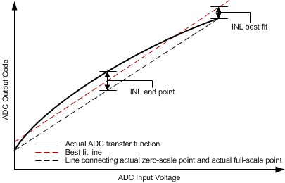
UCD3138128A Best_Fit_INL_End_Point_INL_slusc66.gif Figure 8. Best Fit INL and End Point INL
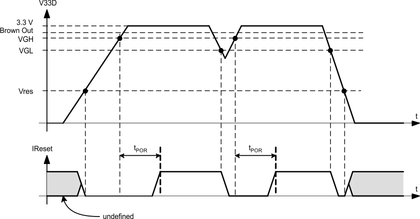
UCD3138128A POR_BOR_slusbz8.gif Figure 9. Power On Reset (POR) / Brown Out Reset (BOR)
VGH – This is the V33A threshold where the internal power is declared good. The UCD3138xA comes out of reset when above this threshold.
VGL – This is the V33A threshold where the internal power is declared bad. The device goes into reset when below this threshold.
Vres This is the V33A threshold where the internal reset signal is no longer valid. Below this threshold the device is in an indeterminate state.
IReset This is the internal reset signal. When low, the device is held in reset. This is equivalent to holding the reset pin on the IC low.
tPOR The time delay from when VGH is exceeded to when the device comes out of reset.
Brown Out – This is the V33A voltage threshold at which the device sets the brown out status bit. In addition an interrupt can be triggered if enabled.

Typical Clock Gating Power Savings

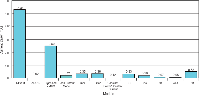
UCD3138128A typical_cloclk_pwr_save3_slusc99.gif

The CLKGATECTRL register provides control bits that can enable or disable the clock to several peripherals such as, PCM, CPCC, digital filters, front ends, DPWMs, UARTs, ADC-12 and more.

By default, all these controls are enabled. If a specific peripheral is not used the clock gate can be disabled in order to block the propagation of the clock signal to that peripheral and therefore reduce the overall current consumption of the device. The power savings chart displays the power savings per module. For example there are 4 DPWM modules, therefore, if all 4 are disabled a total of ~20 mA can be saved.