8 Specifications
8.1 Absolute Maximum Ratings (1)
over operating free-air temperature range (unless otherwise noted)
|
VALUE |
UNIT |
| MIN |
MAX |
|
| V33D |
V33D to DGND |
–0.3 |
3.8 |
V |
| V33DIO |
V33DIO to DGND |
–0.3 |
3.8 |
V |
| V33A |
V33A to AGND |
–0.3 |
3.8 |
V |
| BP18 |
BP18 to DGND |
-0.3 |
2.5 |
V |
| |DGND – AGND| |
Ground difference |
|
0.3 |
V |
| RTC_IN_1_8/RSVD |
|
-0.3 |
3.0 |
V |
| All Pins, excluding AGND(2) |
Voltage applied to any pin |
–0.3 |
3.8 |
V |
| TOPT |
Junction Temperature |
–40 |
125 |
°C |
(1) Stresses beyond those listed under Absolute Maximum Ratings may cause permanent damage to the device. These are stress ratings only, which do not imply functional operation of the device at these or any other conditions beyond those indicated under Recommended Operating Conditions. Exposure to absolute-maximum-rated conditions for extended periods may affect device reliability.
(2) Referenced to DGND
8.2 Handling Ratings
|
MIN |
MAX |
UNIT |
| Tstg |
Storage temperature range |
–55 |
150 |
°C |
| V(ESD) |
Electrostatic discharge |
Human body model (HBM), per ANSI/ESDA/JEDEC JS-001, all pins(1) |
–2000 |
2000 |
V |
| Charged device model (CDM), per JEDEC specification JESD22-C101, all pins(2) |
–500 |
500 |
(1) JEDEC document JEP155 states that 500-V HBM allows safe manufacturing with a standard ESD control process.
(2) JEDEC document JEP157 states that 250-V CDM allows safe manufacturing with a standard ESD control process.
8.3 Recommended Operating Conditions
Over operating free-air temperature range (unless otherwise noted)
|
|
MIN |
TYP |
MAX |
UNIT |
| V33D |
Digital power |
3.0 |
3.3 |
3.6 |
V |
| V33DIO |
Digital I/O power |
3.0 |
3.3 |
3.6 |
V |
| V33A |
Analog power |
3.0 |
3.3 |
3.6 |
V |
| BP18 |
1.8 V digital power |
1.6 |
1.8 |
2.0 |
V |
| TJ |
Junction temperature |
-40 |
- |
125 |
°C |
8.4 Thermal Information
| THERMAL METRIC(1) |
80-PIN QFN |
UNIT |
| RθJA |
Junction-to-ambient thermal resistance |
47.8 |
°C/W |
| RθJCtop |
Junction-to-case (top) thermal resistance |
7.8 |
| RθJB |
Junction-to-board thermal resistance |
24.4 |
| ψJT |
Junction-to-top characterization parameter |
0.2 |
| ψJB |
Junction-to-board characterization parameter |
24.0 |
| RθJCbot |
Junction-to-case (bottom) thermal resistance |
N/A |
(1) For more information about traditional and new thermal metrics, see the
IC Package Thermal Metrics application report,
SPRA953.
8.5 Electrical Characteristics
V33A = V33D = V33DIO = 3.3V; 1μF from BP18 to DGND, TJ = –40°C to 125°C (unless otherwise noted)
| PARAMETER |
TEST CONDITION |
MIN |
TYP |
MAX |
UNIT |
| SUPPLY CURRENT |
|
|
|
|
|
|
I33A(5) |
Measured on V33A. The device is powered up but all ADC12 and EADC sampling is disabled |
|
6.3 |
|
mA |
|
I33DIO(5) |
All GPIO and communication pins are open |
|
0.35 |
|
mA |
|
I33D(5) |
ROM program execution |
|
69 |
|
mA |
|
I33 |
The device is in ROM mode with all DPWMs enabled and switching at 2 MHz. The DPWMs are all unloaded. |
|
93 |
100 |
mA |
| ERROR ADC INPUTS EAP, EAN |
|
EAP – AGND |
|
–0.15 |
|
1.998 |
V |
|
EAP – EAN |
|
–0.256 |
|
1.848 |
V |
|
Typical error range |
AFE = 0 |
–256 |
|
248 |
mV |
|
EAP – EAN Error voltage digital resolution |
AFE = 3 |
0.8 |
1 |
1.20 |
mV |
| AFE = 2 |
1.7 |
2 |
2.30 |
mV |
| AFE = 1 |
3.55 |
4 |
4.45 |
mV |
| AFE = 0 |
6.90 |
8 |
9.10 |
mV |
| REA |
Input impedance (See Figure 9) |
AGND reference |
0.5 |
|
|
MΩ |
| IOFFSET |
Input offset current (See Figure 9) |
|
–5 |
|
5 |
μA |
|
EADC Offset |
Input voltage = 0 V at AFE = 0 |
–16 |
|
16 |
mV |
| Input voltage = 0 V at AFE = 1 |
–10 |
|
10 |
mV |
| Input voltage = 0 V at AFE = 2 |
–6 |
|
-6 |
mV |
| Input voltage = 0 V at AFE = 3 |
–4 |
|
4 |
mV |
|
Sample Rate |
|
|
|
15.625 |
MHz |
|
Analog Front End Amplifier Bandwidth |
|
|
100 |
|
MHz |
| A0 |
Gain |
See Figure 10 |
|
1 |
|
V/V |
| Minimum output voltage |
|
|
|
21 |
mV |
| EADC DAC |
|
DAC range |
|
0 |
|
1.6 |
V |
|
VREF DAC reference resolution |
10 bit, No dithering enabled |
|
1.56 |
|
mV |
|
VREF DAC reference resolution |
With 4 bit dithering enabled |
|
97.6 |
|
μV |
|
INL |
|
–1.5 |
|
1.5 |
LSB |
|
DNL |
|
–1.0 |
|
2.1 |
LSB |
|
DAC reference voltage |
|
1.58 |
|
1.61 |
V |
| ADC12 |
| IBIAS |
Bias current for PMBus address pins |
|
9.5 |
|
10.5 |
μA |
|
Measurement range for voltage monitoring |
|
0 |
|
2.5 |
V |
|
Internal ADC reference voltage |
–40°C to 125°C |
2.475 |
2.500 |
2.53 |
V |
|
Change in Internal ADC reference from 25°C reference voltage(5) |
–40°C to 25°C |
|
–0.7 |
|
mV |
| 25°C to 125°C |
-6 |
|
|
|
ADC12 INL integral nonlinearity(5) |
ADC_SAMPLING_SEL = 6 for all ADC12 data, 25 °C to 125 °C |
|
-7.5/+2.9 |
|
LSB |
|
ADC12 DNL differential nonlinearity(5) |
|
–0.7/+3.2 |
|
LSB |
|
ADC Zero Scale Error |
–7 |
±5 |
7 |
mV |
|
ADC Full Scale Error |
–35 |
±20 |
35 |
mV |
|
Input bias |
2.5 V applied to pin |
|
|
200 |
nA |
|
Input leakage resistance(5) |
ADC_SAMPLING_SEL= 6 or 0 |
|
1 |
|
MΩ |
|
Input Capacitance(5) |
|
|
10 |
|
pF |
| DIGITAL INPUTS/OUTPUTS(1)(2) |
| VOL |
Low-level output voltage(3) |
IOH = 4 mA, V33DIO = 3 V |
|
|
DGND
+ 0.25 |
V |
| VOH |
High-level output voltage (3) |
IOH = –4 mA, V33DIO = 3 V |
V33DIO – 0.6 |
|
|
V |
| VIH |
High-level input voltage |
V33DIO = 3 V |
2.1 |
|
|
V |
| VIL |
Low-level input voltage |
V33DIO = 3 V |
|
|
1.1 |
V |
| IOH |
Output sinking current |
|
|
|
4 |
mA |
| IOL |
Output sourcing current |
|
–4 |
|
|
mA |
| SYSTEM PERFORMANCE |
|
Processor master clock (MCLK) |
|
|
31.25 |
|
MHz |
| tDelay |
Digital filter delay(4) |
(1 clock = 32ns) |
|
|
6 |
MCLKs |
| f(PCLK) |
Internal oscillator frequency |
|
240 |
250 |
260 |
MHz |
| ISHARE |
Current share current source (See Figure 28) |
|
238 |
|
259 |
μA |
| RSHARE |
Current share resistor (See Figure 28) |
|
9.7 |
|
10.3 |
kΩ |
| POWER ON RESET AND BROWN OUT (V33A pin, See Figure 3) |
| VGH |
|
Voltage good High |
|
2.7 |
|
V |
| VGL |
|
Voltage good Low |
|
2.5 |
|
V |
| Vres |
Voltage at which IReset signal is valid(5) |
|
|
0.8 |
|
V |
|
Brownout |
Internal signal warning of brownout conditions |
|
2.9 |
|
V |
| TEMPERATURE SENSOR(5) |
| VTEMP |
|
Voltage range of sensor |
1.46 |
|
2.44 |
V |
|
Voltage resolution |
Volts/°C |
|
6.3 |
|
mV/ºC |
|
Temperature resolution |
Degree C per bit |
|
0.0969 |
|
ºC/LSB |
|
Accuracy(5)(6) |
-40°C to 125°C |
–10 |
±5 |
10 |
ºC |
|
Temperature range |
-40°C to 125°C |
–40 |
|
125 |
ºC |
| ITEMP |
|
Current draw of sensor when active |
|
30 |
|
μA |
| VAMB |
Ambient temperature |
Trimmed 25°C reading |
|
1.87 |
|
V |
| ANALOG COMPARATOR |
| DAC |
Reference DAC Range |
|
0 |
|
2.5 |
V |
|
Reference Voltage |
|
2.478 |
2.5 |
2.513 |
V |
|
Bits |
|
|
7 |
|
bits |
|
INL(5) |
|
–0.42 |
|
0.21 |
LSB |
|
DNL(5) |
|
0.06 |
|
0.12 |
LSB |
|
Offset |
|
–5.5 |
|
19.5 |
mV |
|
Reference DAC buffered output load(7) |
|
0.5 |
|
1 |
mA |
|
Buffer offset (-0.5 mA) |
|
|
|
8.3 |
mV |
|
Buffer offset (1.0 mA) |
|
|
|
17 |
mV |
| RTC INTERFACE |
| fRTC |
RTC external input frequency |
|
|
10 |
|
MHz |
(1) DPWM outputs are low after reset. Other GPIO pins are configured as inputs after reset.
(2) On the 40 pin package V33DIO is connected to V33D internally.
(3) The maximum total current, IOHmax and IOLmax for all outputs combined, should not exceed 12 mA to hold the maximum voltage drop specified. Maximum sink current per pin = –6 mA at VOL; maximum source current per pin = 6 mA at VOH.
(4) Time from close of error ADC sample window to time when digitally calculated control effort (duty cycle) is available. This delay, which has no variation associated with it, must be accounted for when calculating the system dynamic response.
(5) Characterized by design and not production tested.
(6) Ambient temperature offset value from the TEMPSENCTRL register should be used to meet accuracy.
(7) Available from reference DACs for comparators D, E, F and G.
8.6 Timing Characteristics
V33A = V33D = V33DIO = 3.3V; 1μF from BP18 to DGND, TJ = –40°C to 125°C (unless otherwise noted)
| PARAMETER |
TEST CONDITION |
MIN |
TYP |
MAX |
UNIT |
| EADC DAC |
| t |
Settling Time |
From 10% to 90% |
|
250 |
|
ns |
| ADC12 |
|
ADC single sample conversion time(2) |
ADC_SAMPLING_SEL= 6 or 0 |
|
3.9 |
|
μs |
| SYSTEM PERFORMANCE |
| TWD |
Watchdog time out resolution |
Total time is: TWD x (WDCTRL.PERIOD+1) |
10.5 |
13.3 |
17 |
ms |
|
Time to disable DPWM output based on active FAULT pin signal |
High level on FAULT pin |
|
66 |
|
ns |
|
Flash Read |
|
|
1 |
|
MCLKs |
| tDelay |
Digital filter delay(1) |
(1 clock = 32ns) |
|
|
6 |
MCLKs |
|
Retention period of flash content (data retention and program) |
TJ = 25°C |
100 |
|
|
years |
|
Program time to erase one page or block in data flash or program flash |
|
|
20 |
|
ms |
|
Program time to write one word in program flash |
|
|
50 |
|
µs |
|
Program time to write one word in data flash |
|
|
40 |
|
µs |
|
Sync-in/sync-out pulse width |
Sync pin |
|
256 |
|
ns |
| POWER ON RESET AND BROWN OUT (V33A pin, See Figure 3) |
| tPOR |
|
Time delay after Power is good or RESET* relinquished |
|
1 |
|
ms |
| tEXC1 |
The time it takes from the device to exit a reset state and begin executing the boot flash.(2) |
IRESET goes from a low state to a high state. This is approximately equivalent to toggling the external reset pin from low to high state. |
|
0.5 |
|
ms |
| tEXC2 |
The time it takes from the device to exit a reset state and begin executing program flash bank 0 (32 kB).(2) |
IRESET goes from a low state to a high state. This is approximately equivalent to toggling the external reset pin from low to high state. |
|
3 |
|
ms |
| tEXCT |
The time it takes from the device to exit a reset state and begin executing the total program flash (64 kB).(2) |
IRESET goes from a low state to a high state. This is approximately equivalent to toggling the external reset pin from low to high state. |
|
6 |
|
ms |
| TEMPERATURE SENSOR(2) |
| tON |
|
Turn on time / settling time of sensor |
|
100 |
|
μs |
| ANALOG COMPARATOR |
|
Bits |
|
|
7 |
|
bits |
|
INL(2) |
|
–0.42 |
|
0.21 |
LSB |
|
DNL(2) |
|
0.06 |
|
0.12 |
LSB |
|
Time to disable DPWM output based on 0 V to 2.5 V step input on the analog comparator.(2) |
|
|
90 |
150 |
ns |
(1) Time from close of error ADC sample window to time when digitally calculated control effort (duty cycle) is available. This delay, which has no variation associated with it, must be accounted for when calculating the system dynamic response.
(2) Characterized by design and not production tested.
8.7 PMBUS/SMBUS/IC Timing2
The timing characteristics and timing diagram for the communications interface that supports I2C, SMBus, and PMBus in Slave or Master mode are shown in the Timing Requirements, Figure 1, and Figure 2. The numbers in the Timing Requirements are for 400 kHz operating frequency. However, the device supports two speeds, standard (100 kHz) and fast (400 kHz).
8.8 Timing Requirements
| PARAMETER |
TEST CONDITIONS |
MIN |
TYP |
MAX |
UNIT |
| Typical values at TA = 25°C and VCC = 3.3 V (unless otherwise noted) |
| fSMB |
SMBus/PMBus operating frequency |
Slave mode, SMBC 50% duty cycle |
|
100 |
400 |
kHz |
| fI2C |
I2C operating frequency |
Slave mode, SCL 50% duty cycle |
|
100 |
400 |
kHz |
| t(BUF) |
Bus free time between start and stop(5) |
|
|
1.3 |
|
µs |
| t(HD:STA) |
Hold time after (repeated) start(5) |
|
|
0.6 |
|
µs |
| t(SU:STA) |
Repeated start setup time(5) |
|
|
0.6 |
|
µs |
| t(SU:STO) |
Stop setup time(5) |
|
|
0.6 |
|
µs |
| t(HD:DAT) |
Data hold time |
Receive mode |
|
0 |
|
ns |
| t(SU:DAT) |
Data setup time |
|
|
100 |
|
ns |
| t(TIMEOUT) |
Error signal/detect(1) |
|
|
|
35 |
ms |
| t(LOW) |
Clock low period |
|
1.3 |
|
|
µs |
| t(HIGH) |
Clock high period(2) |
|
|
|
35 |
ms |
| t(LOW:SEXT) |
Cumulative clock low slave extend time(3) |
|
|
|
25 |
ms |
| tf |
Clock/data fall time |
Rise time tr = (VILmax – 0.15) to (VIHmin + 0.15) |
20 + 0.1 Cb(4) |
|
300 |
ns |
| tr |
Clock/data rise time |
Fall time tf = 0.9 VDD to (VILmax – 0.15) |
20 + 0.1 Cb(4) |
|
300 |
ns |
| Cb |
Total capacitance of one bus line |
|
|
|
400 |
pF |
(1) The device times out when any clock low exceeds t(TIMEOUT).
(2) t(HIGH), Max, is the minimum bus idle time. SMBC = SMBD = 1 for t > 50 ms causes reset of any transaction that is in progress. This specification is valid when the NC_SMB control bit remains in the default cleared state (CLK[0] = 0).
(3) t(LOW:SEXT) is the cumulative time a slave device is allowed to extend the clock cycles in one message from initial start to the stop.
(4) Cb (pF)
(5) Fast mode, 400 kHz
 Figure 1. IC/SMBUS/PMBUS Timing Diagram2
8.9 Power On Reset (POR) / Brown Out Detect (BOD)
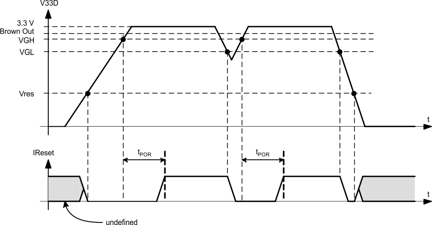 Figure 3. Power On Reset (POR) / Brown Out Reset (BOR)
| VGH – |
This is the V33A threshold where the internal power is declared good. The UCD3138x comes out of reset when above this threshold. |
| VGL – |
This is the V33A threshold where the internal power is declared bad. The device goes into reset when below this threshold. |
| Vres – |
This is the V33A threshold where the internal reset signal is no longer valid. Below this threshold the device is in an indeterminate state. |
| IReset – |
This is the internal reset signal. When low, the device is held in reset. This is equivalent to holding the reset pin on the IC low. |
| tPOR – |
The time delay from when VGH is exceeded to when the device comes out of reset. |
| Brown Out – |
This is the V33A voltage threshold at which the device sets the brown out status bit. In addition an interrupt can be triggered if enabled. |
8.10 Typical Clock Gating Power Savings
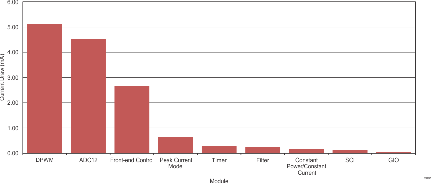
The CLKGATECTRL register provides control bits that can enable or disable the clock to several peripherals such as, PCM, CPCC, digital filters, front ends, DPWMs, UARTs, ADC-12 and more.
By default, all these controls are enabled. If a specific peripheral is not used the clock gate can be disabled in order to block the propagation of the clock signal to that peripheral and therefore reduce the overall current consumption of the device. The power savings chart displays the power savings per module. For example there are 4 DPWM modules, therefore, if all 4 are disabled a total of ~20 mA can be saved.
8.11 Typical Characteristics
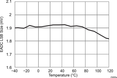
 Figure 4. EADC LSB Size With 4x Gain (Mv) vs. Temperature
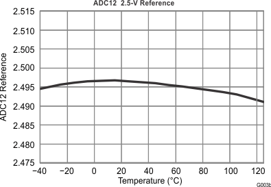
 Figure 6. ADC12 2.5-V Reference vs. Temperature
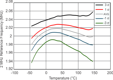
 Figure 8. Oscillator Frequency (2MHz Reference, Divided Down From 250MHz) vs. Temperature
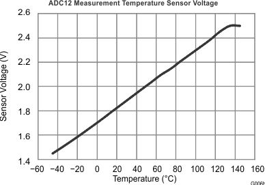
 Figure 5. ADC12 Measurement Temperature Sensor Voltage vs. Temperature
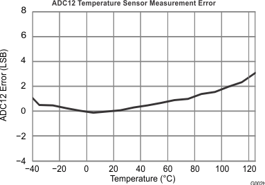
 Figure 7. ADC12 Temperature Sensor Measurement Error vs. Temperature
 Figure 1. IC/SMBUS/PMBUS Timing Diagram2
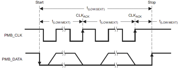 Figure 2. Bus Timing In Extended Mode
 Figure 3. Power On Reset (POR) / Brown Out Reset (BOR)
