ZHCSCD4B July 2013 – August 2014 UCC28910
PRODUCTION DATA.
- 1 特性
- 2 应用范围
- 3 说明
- 4 简化电路原理图 简化电路原理图
- 5 修订历史记录
- 6 Terminal Configuration and Functions
- 7 Specifications
-
8 Detailed Description
- 8.1 Overview
- 8.2 Functional Block Diagram
- 8.3 Detailed Device Description
- 8.4 Feature Description
- 8.5 Device Functional Modes
-
9 Applications and Implementation
- 9.1 Application Information
- 9.2
Typical Application
- 9.2.1
Battery Charger, 5 V, 6 W
- 9.2.1.1 Design Requirements
- 9.2.1.2
Detailed Design Procedure
- 9.2.1.2.1 Power Handling Curves
- 9.2.1.2.2 Definition of Terms
- 9.2.1.2.3 Maximum Target Switching Frequency
- 9.2.1.2.4 Transformer Turns Ratio, Inductance, Primary-Peak Current
- 9.2.1.2.5 Bulk Capacitance
- 9.2.1.2.6 Output Capacitance
- 9.2.1.2.7 VDD Capacitance, CVDD
- 9.2.1.2.8 VS Resistor Divider
- 9.2.1.2.9 RVDD Resistor and Turn Ratio
- 9.2.1.2.10 Transformer Input Power
- 9.2.1.2.11 RIPK Value
- 9.2.1.2.12 Primary Inductance Value
- 9.2.1.2.13 Pre-Load
- 9.2.1.2.14 DRAIN Voltage Clamp Circuit
- 9.2.1.3 Application Curves
- 9.2.1.4 Average Efficiency Performance and Standby Power of the UCC28910FBEVM-526
- 9.2.1
Battery Charger, 5 V, 6 W
- 10Power Supply Recommendations
- 11Layout
- 12器件和文档支持
- 13机械封装和可订购信息
8 Detailed Description
8.1 Overview
The device is an HV switcher dedicated to an off-line power supply in an isolated flyback configuration. HV switcher means that device integrates the power switch, a 700-V power FET, with the control logic. The control logic controls both the output voltage and the output current without the need of an optical coupler. This control method is known as Primary-Side Regulation (PSR) and it operates by analyzing the voltage waveform on the auxiliary winding of the transformer. This allows significant cost saving with respect to traditional control scheme that uses an optical coupler. The transformer auxiliary winding is also used to provide housekeeping supply power to the control logic. The device operates in Constant Voltage mode (CV) when it is controlling the output voltage. The device operates in Constant Current mode (CC) when the output current is controlled. The device operates in CV mode or in CC mode according to the load condition. (See Figure 18). The control algorithm that implements both, modulation of the switching frequency and the amplitude modulation of the primary current peak, allows the power supply to operate efficiently over the entire load range. The high-voltage current source used for startup is kept off during normal operation thereby minimizing standby power consumption. The device also incorporates a smart power management to minimize its current consumption from the VDD terminal. This power consumption is reduced when the converter is lightly loaded or unloaded allowing for a total input power of less than 30 mW when converter input voltage is 265 VAC and unloaded. A number of protection features inside the device allow for improved overall system reliability.
8.2 Functional Block Diagram
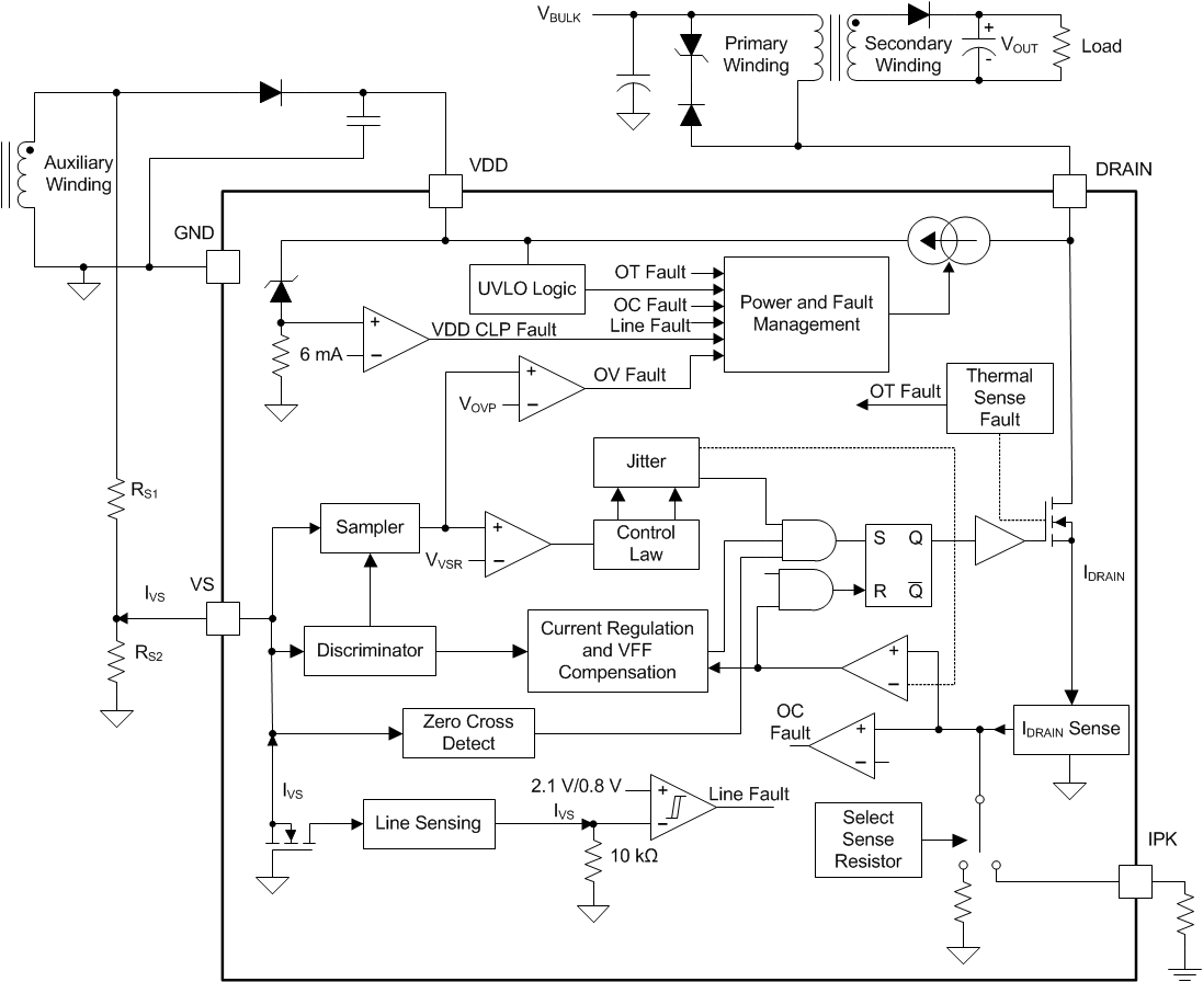
8.3 Detailed Device Description
8.3.1 VDD (Device Voltage Supply)
The VDD terminal is connected to a bypass capacitor to ground and typically to a rectifier diode connected to the auxiliary winding. The VDD turn on UVLO threshold is 9.5 V (VDDON typical) and turn off UVLO threshold is 6.5 V (VDDOFF typical). The terminal is provided with an internal clamp that prevents the voltage from exceeding the absolute maximum rating of the terminal. The internal clamp cannot absorb currents higher than 10 mA (see IVDD(clp) in Absolute Maximum Ratings), to avoid damaging the device, when the clamp flowing current exceeds 6 mA (IDDCLP_OC typical) the device stops switching. The VDD terminal operating range is then from 7 V (VDDOFF maximum) up to 26 V (VDDCLAMP minimum). The USB charging specification requires that the output current operates in constant current mode from 5 V to a minimum of 2 V; this is easily achieved with a nominal VDD of approximately 17 V. Set NAS (auxiliary-to-secondary windings turn ratio) to 17 V / (VOUT + VF) where VF is the voltage drop on the output diode at low current. The additional VDD headroom up to the clamp allows for VDD to rise due to the leakage energy delivered to the VDD in high-load conditions.
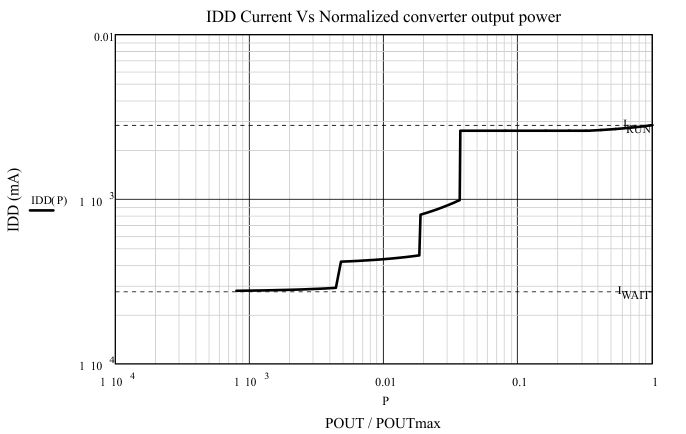 Figure 13. VDD Current Consumption
8.3.2 GND (Ground)
The device is provided with three terminals, shorted together, that are used as external ground reference to the controller for analog signal reference. The three terminals function to pull out the heat caused by the power dissipation of the internal power FET. Place the VDD bypass capacitor close to GND and VDD with short traces to minimize noise on the VS and IPK signal terminals.
8.3.3 VS (Voltage Sense)
The VS terminal is connected to a resistor divider from the auxiliary winding to ground. The VS terminal provides three functions.
- It provides output voltage information to the voltage control Loop. The output voltage feedback information is sampled at the end of the transformer secondary current demagnetization time to provide an accurate representation of the output voltage.
- It also provides timing information to achieve valley switching and the duty cycle of the secondary transformer current is determined by the waveform on the VS terminal.
- It samples the bulk capacitor input voltage providing under-voltage shutdown.
The data provided in 1) and 2) are sensed during the MOSFET off-time; 3) is performed during the MOSFET on-time when the auxiliary-winding voltage is negative.
During MOSFET on-time, the voltage on VS terminal is clamped to GND and through the resistance RS1 connected between the auxiliary winding and VS. During the on-time, the current sourced from the VS terminal is sensed by the device. For the under-voltage function, the enable threshold on VS current is 210 μA and the disable threshold is 75 μA.
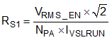
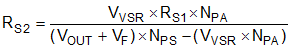
The resistor values for RS1 and RS2 can be determined by the equations below.
where
where
8.3.4 IPK (Set the Maximum DRAIN Current Peak)
A resistance (RIPK) connected between IPK terminal and GND sets the maximum value of the power FET peak current. A current, ISENSE, proportional to the power FET current comes out from the IPK terminal during power FET on time.

where

The voltage across RIPK is fed to the PWM comparator and established to switch off the power FET according to the following equation:
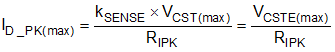
where

If the terminal is shorted to GND (RIPK = 0) the peak current is automatically set to 600 mA (ID_PEAK(max)).
A test is performed at device start up to check whether the IPK terminal is shorted to GND or the RIPK is present. If RIPK is less than RIPK_SHORT (maximum), the device interprets it as a short (RIPK = 0) and the DRAIN peak current is set to ID_PEAK(max). Otherwise, if RIPK is greater than RIPK(min) (minimum), the device sets the peak current DRAIN according to the previous equation. A value of RIPK that is in between the before said values, is not allowed since the value of the peak current may be selected using anyone of the two sense resistances: the internal sense resistance and RIPK.
8.3.5 DRAIN
The DRAIN terminal is connected to the DRAIN of the internal power FET. This terminal also provides current to the high voltage current source at start up.
8.4 Feature Description
The UCC28910 is a flyback power-supply switcher which provides accurate output voltage and constant current regulation with primary-side feedback, eliminating the need for optical coupler feedback circuits. The device has an internal 700-V power FET plus a controller which forces the converter to operate in discontinuous conduction mode with valley switching to minimize switching losses. The modulation scheme is a combination of frequency and primary-peak current modulation to provide optimized conversion efficiency over the entire load range. The control law provides a wide dynamic operating range to achieve less than 30-mW standby power.
The UCC28910 includes features in the modulator to reduce the EMI peak energy of the fundamental switching frequency and harmonics. Accurate voltage and constant current regulation, fast dynamic response, and fault protection are achieved with primary-side control.
A complete charger solution can be realized with a straightforward design process, low cost and low component count solution.
8.4.1 Primary-Side Voltage Regulation
Figure 14 illustrates a flyback converter. The voltage regulation blocks of the device are shown. The power train operation is the same as any DCM flyback circuit but accurate output voltage and current sensing is the key to primary side control.
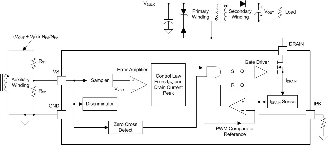 Figure 14. Voltage Loop Block Diagram
In primary-side control, the output voltage is sensed by the auxiliary winding during the transfer of transformer energy to the secondary. Figure 15 shows the down slope representing a decreasing total rectifier VF and the secondary winding resistance voltage drop as the secondary current decreases to 0 A. To achieve an accurate representation of the secondary output voltage on the auxiliary winding, the Discriminator Block (Figure 14) reliably ignores the leakage inductance reset and ring, continuously samples the auxiliary voltage during the down slope after the ringing is diminished, and captures the error signal at the time the secondary winding reaches 0 current. The internal reference on VS is 4 V; the resistor divider is selected as outlined in the VS terminal description.
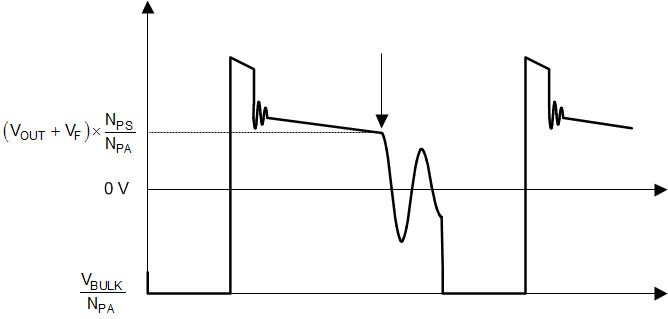 Figure 15. Auxiliary Winding Voltage
The UCC28910 VS signal Discriminator Block (Figure 14) ensures accurate sampling time for an accurate sample of the output voltage from the auxiliary winding. There are however some details of the auxiliary winding signal to ensure reliable operation, specifically the reset time of the leakage inductance and the duration of any subsequent leakage inductance ring. Refer to Figure 16 for a detailed illustration of waveform criteria to ensure a reliable sample on the VS terminal. The first detail to examine is the duration of the leakage inductance reset pedestal, tLK_RESET. Since this can mimic the waveform of the secondary current decay, followed by a sharp down-slope, it is important to keep the leakage reset time less than 500 ns for IDRAIN minimum, and less than 1.5 μs for IDRAIN maximum. The second detail is the amplitude of ringing on the auxiliary winding waveform (VAUX) following tLK_RESET. The peak-to-peak voltage at the VS terminal should be less than approximately 100 mVp-p at least 200 ns before the end of the demagnetization time, tDMAG. If there is a concern with excessive ringing, it usually occurs during light or no-load conditions, when tDMAG is at the minimum. The tolerable ripple on VS is scaled up to the auxiliary winding voltage by RS1 and RS2, and is equal to 100 (RS1 + RS2) / RS2 mV.
 Figure 16. VS Voltage
During voltage regulation, the controller operates in frequency modulation mode and amplitude modulation mode. The internal operating frequency limits of the controller are 115 kHz maximum and 420 Hz minimum. The transformer primary inductance and turns ratio sets the maximum operating frequency of the converter. The output preload resistor and efficiency at low power determines the converter minimum operating frequency. There is no external compensation required for the UCC28910 device.
8.4.2 Primary-Side Current Regulation
Timing information at the VS terminal and the primary current information allow accurate regulation of the secondary average current. The control law dictates that as power is increased in CV regulation and approaching CC regulation the primary-peak current is at ID_PK(max) = VCSTE(max) / RIPK. Referring to Figure 17, the primary-peak current, turns ratio, secondary demagnetization time (tDMAG), and switching period (tSW) establish the secondary average output current. When the average output current reaches the regulation reference in the current control block, the controller operates in frequency modulation mode to control the output current at any output voltage at or below the voltage regulation target as long as the aux winding can keep VDD above the VDD UVLO threshold (VDDOFF).
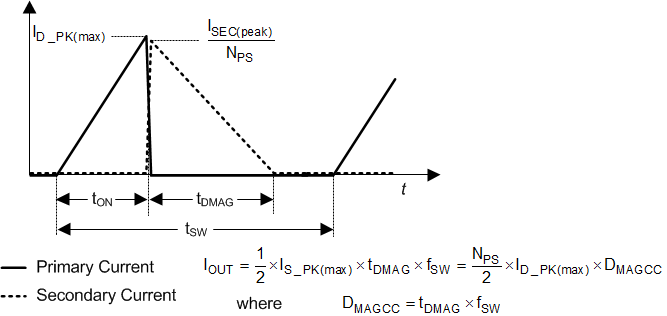 Figure 17. Output Current Estimation
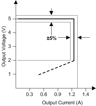 Figure 18. Target Output V-I Characteristic
KCC is defined as the maximum value of the secondary-side conduction duty cycle. It is set internally by the UCC28910 and occurs during constant current control mode.
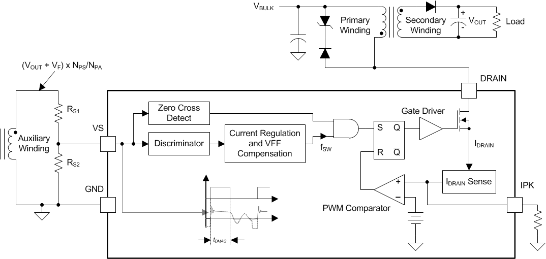 Figure 19. Output Current Control Loop Block Diagram
8.4.3 Voltage Feed Forward Compensation
During normal operation the on-time is determined by sensing the power FET current and switching off the power FET as this current reaches a threshold fixed by the feedback loop according to the load condition. The power FET is not immediately turned off and its current, that is also the primary winding current, continues to rise for some time during the propagation delay (tDELAY in Figure 20). Keeping the reference for the PWM comparator constant, the value of the primary winding peak current depends on the slope of the primary winding current and tDELAY.
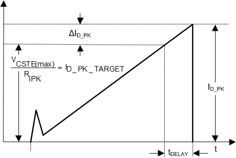 Figure 20. Propagation Delay Effect on the Primary Current Peak
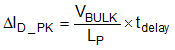
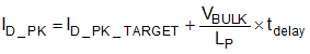
The current loop estimates the output current assuming the primary winding peak current is equal to the IPK_TARGET and compares this estimated current with a reference to obtain the current regulation. Considering, ID_PEAK is different from ID_PEAK_TARGET (see Figure 20) we need to compensate the effect of the propagation delay. The UCC28910 incorporates fully integrated propagation delay compensation that modifies the switching frequency keeping the output current constant during (CC) Constant Current Mode operation. This function is integrated in the controller and requires no external components. This feature keeps the output current constant despite input voltage variations and primary inductance value spread.
8.4.4 Control Law
During voltage regulation, the device operates in switching frequency modulation mode and primary current peak amplitude modulation mode. The internal operating frequency limits of the device are fSW(max) and fSW(min). The transformer primary inductance and primary-peak current chosen sets the maximum operating frequency of the converter. The output preload resistor and efficiency at low power determines the converter minimum operating frequency. During constant current regulation the device operates only in frequency modulation mode reducing the switching frequency as the output voltage decreases. Figure 21 shows how the primary peak current and the switching frequency change with respect to changes in load.
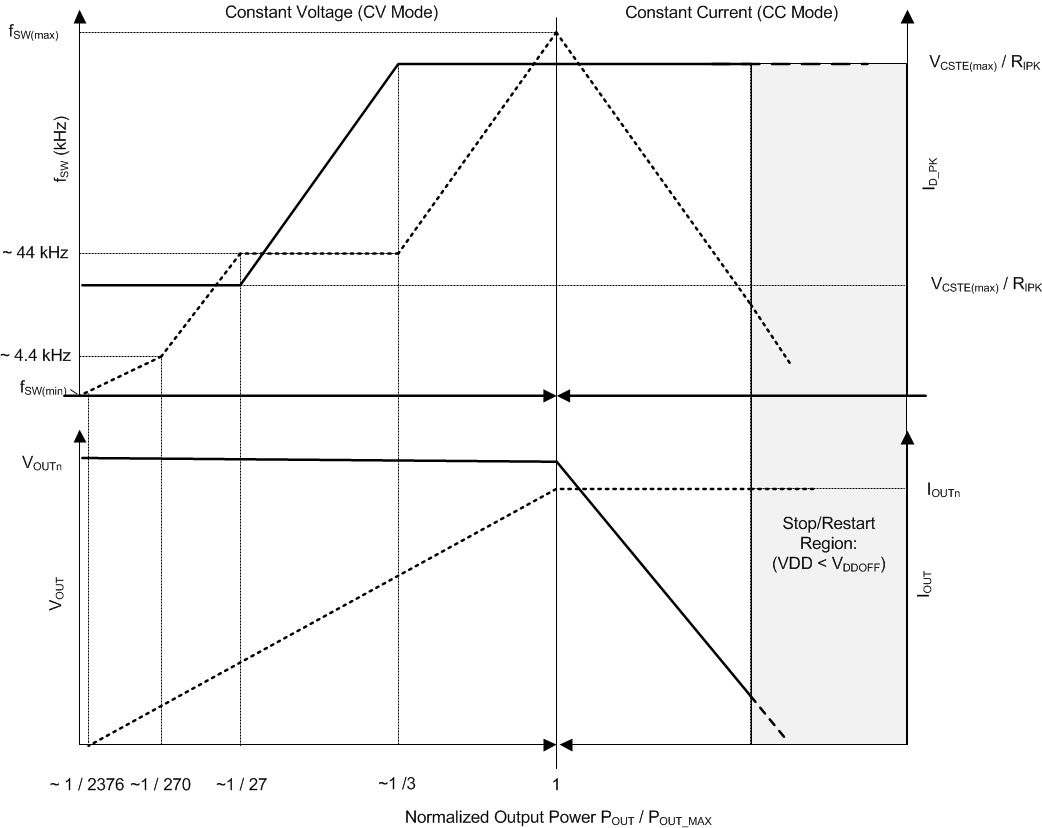 Figure 21. Control Law Profile
8.4.5 Valley Switching
The UCC28910 utilizes valley switching to reduce switching losses in the MOSFET and minimize the turn on FET current spike. The UCC28910 operates in valley switching in almost all load conditions until the VDS ringing is diminished. By switching at the lowest VDS voltage the MOSFET turn on dV / dt is minimized which is a benefit to reduce EMI.
Referring to Figure 22, the UCC28910 operates in a valley skipping mode in most load conditions to maintain an accurate voltage regulation point and still switch on the lowest available VDS voltage.
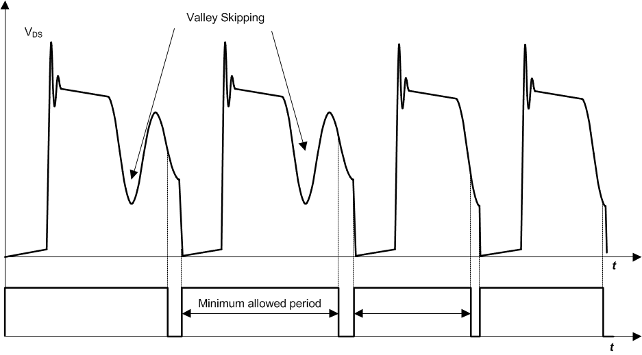 Figure 22. Valley Skipping
Valley switching is maintained during constant current regulation to provide improved efficiency and EMI benefits in constant current operation.
In very light-load or no-load condition the VDS ringing is very low and not easy to detect, moreover with very low ringing amplitude there would be no benefit in valley switching so in this condition the valley switching is disabled (see Figure 23).
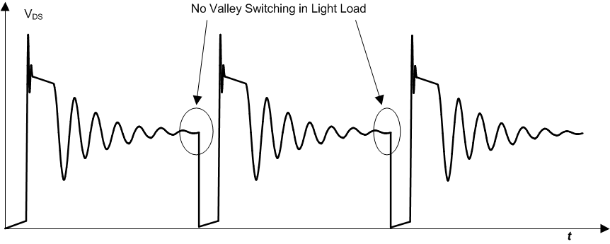 Figure 23. Valley Switching Disable at Light Load
8.4.6 Startup Operation
UCC28910 is provided with a high-voltage current source, connected between the DRAIN terminal and the VDD terminal; this current source is activated when a voltage is applied on DRAIN terminal. The current source charges the capacitor connected between VDD and GND increasing the VDD voltage. As VDD exceeds VDDON the current source is turned off and the controller internal logic is activated and the device starts switching. If the VDD voltage falls below the VDDOFF threshold, or a fault condition is detected, the controller stops operation and its current consumption is reduced to ISTART or IFAULT. The high-voltage current source is turned on again when VDD voltage goes below VDDHV(on) (see Figure 11 for reference).
The initial three cycles are limited to ID_PEAK(max) / 3. This allows sensing any input or output faults with minimal power delivery. After the initial three cycles at ID_PEAK(max) / 3, the controller responds to the condition dictated by the control law.
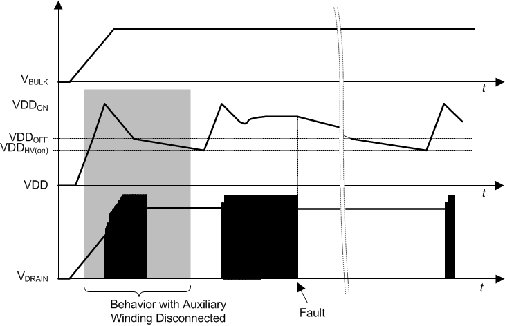 Figure 24. Start Up and Auto Re-Start Operation
The converter remains in DCM during charging of the output capacitor(s), and operates in constant current mode until the output voltage is in regulation.
To avoid high-power dissipation inside the device, such as in the event that VDD is accidentally shorted to GND, the current provided by the high-voltage current source is reduced (ICH1) until VDD < 1 V (typical).
8.4.7 Fault Protection
There is comprehensive fault protection incorporated into the UCC28910. Protection functions include:
- Output Over-Voltage Fault
- Input Under-Voltage Fault
- Internal Over-Temperature Fault
- Primary Over-Current Fault
- Maximum tON Fault
- VDD Clamp Over Current
8.4.7.1 Output Over-Voltage
The output over-voltage function is determined by the voltage feedback on the VS terminal. If the voltage sample on VS exceeds 4.6 V, which correlates to 115% of nominal VOUT, the device stops switching and reduces its current consumption to IFAULT, slowly discharging the VDD capacitor to the VDDHV(on) threshold. At this time the standard startup sequence begins. The initial three cycles of startup at low-peak DRAIN current is important to monitor VOUT and deliver minimal power. The reset and restart, or hiccup, sequence applies for all fault protection. The slow VDD capacitor discharge after a fault allows the high voltage current source to have a low duty cycle to avoid over heating of the device if a fault condition is continuously present resulting in a repetitious start up sequence.
8.4.7.2 Input Under-Voltage
The input under voltage is determined by current information on the VS terminal during the MOSFET on time. The VS terminal is clamped close to GND during the MOSFET on time; at this time the current though RS1 is monitored to determine a sample of the bulk capacitor voltage. The under voltage shutdown current on VS is 75 μA; the enable current threshold is 210 μA. The device must sense the under-voltage condition for three consecutive switching cycles to recognize it as a fault condition. After an under-voltage fault, the same sequence described for output overvoltage occurs.
8.4.7.3 Internal Over-Temperature
The internal over-temperature protection threshold is 150°C with a hysteresis of 50°C. If an over temperature is detected the device stops switching and the current consumption is reduced to IFAULT. The VDD voltage decreases to VDDHV(on) where the high-voltage current source is activated and the VDD voltage rises again until VDDON, where the internal logic is re-activated. If the temperature of the device is not dropped below approximately 100°C (150°C – 50°C) no switching cycles occur and the fault condition is maintained and the current consumption is again IFAULT. For diagnostic purposes, when a thermal shutdown occurs, a short voltage pulse whose amplitude is around 2 V is transmitted on the IPK terminal.
8.4.7.4 Primary Over-Current
The UCC28910 always operates with cycle-by-cycle primary current control. The normal operating range for the peak DRAIN current depends on the resistance (RIPK) connected between the IPK terminal and the GND terminal. The peak DRAIN current should not exceed ID_PEAK(max) even if the IPK terminal is shorted to GND, or should not exceed VCSTE / RIPK if the IPK terminal is tied to GND with the resistance RIPK. There are different reasons the DRAIN current can go out of control, for example a secondary winding short or hard saturation of the transformer. To avoid over-stress of the power FET additional protections are added. If the DRAIN current exceeds IDOCP (~33% higher than ID_PEAK(max)), such as when IPK terminal is shorted to GND, or VCSTE_OCP / RIPK, (VCSTE_OCP ~33% higher than VCSTE(max)), and the condition is sensed for three consecutive switching cycles, a fault shutdown and retry sequence, detailed in the output overvoltage fault description, occurs. If the DRAIN current exceeds a second level of current (VCSTE_OCP2 / RIPK) it is not necessary to detect the fault for three consecutive switching cycles, the device will stop switching immediately.
8.4.7.5 Maximum tON
An additional protection that limits the power FET on time was added. A timer sets a maximum tON time that is proportional to the ID_PEAK value established by the control law. When ID_PEAK is maximum the maximum tON is tONMAX(max) (18 μs typical) if ID_PEAK is minimum the maximum tON is tONMAX(min). (6 μs typical). As the maximum tON is elapsed the power FET is switched off (if it is still on). If for three consecutive switching cycles the power FET is switched off by the maximum tON protection, the device stops switching and sets the consumption low (IVDDFAULT) until the next restart.
8.4.7.6 VDD Clamp Over-Current
The VDD terminal is provided with an internal clamp to prevent the terminal voltage from exceeding the absolute maximum rating. If the current in the clamp exceeds 6 mA (typical), in order to avoid any damage to the device and to the system, a fault condition is assumed and the device stops operation.
8.5 Device Functional Modes
According to the input voltage, the VDD voltage, and the load conditions, the device can operate in different modes:
- At start-up with VDRAIN > 20 V, VDD = 0 V, the HV voltage current source is ON and starts to charge the capacitor connected to the VDD pin. With VDD < 1 V the current provided is limited < 500 µA and VDD rises slowly.
- When VDD exceeds 1 V (VDD < VDDON) the HV current source provides higher current and VDD rises faster.
- When VDD exceeds VDDON the device starts switching and delivers power to its output. According to its load, the converter operates in CV mode or in CC mode.
- CV mode means that the converter keeps the output voltage constant. This operating mode takes place when RLOAD > VOCV / IOCC where VOCV is the target for output voltage and IOCC is the maximum converter output current. In this condition the converter output voltage VOUT = VOCV and the converter output current IOUT < IOCC.
- CC mode means that the converter keeps the output current constant. This operating mode takes place when RLOAD < VOCV / IOCC. In this condition the converter output voltage VOUT < VOCV and the converter output current IOUT = IOCC.
- Device operations can be stopped because of the events listed below:
- If VDD drops below VDDOFF, the device stops switching and its current consumption is lowered to ISTART. Because the converter is not switching, no energy is delivered from the auxiliary winding, the HV current source is off, then the VDD capacitor is discharged with ISTART current.
- If a fault is detected device stops switching and its current consumption is lowered to IFAULT that slowly discharges the VDD capacitor down to VDDOFF where the current consumption is ISTART < IFAULT and the VDD capacitor continues to discharge.
- After the device stops switching, because of 4a or 4b, the VDD voltage drops, when it goes below VDDHV(on), the HV current source is turned on recharging the VDD capacitor up to VDDON.
- When a fault condition is permanently present, the device operates in auto restart-mode. This means that a fault condition is detected, the device stops operation as described in 4b, then VDD drops down to VDDHV(on) when the device start-up sequence takes place. At device turn-on, the fault is again detected and the cycle repeats.