ZHCSCD4B July 2013 – August 2014 UCC28910
PRODUCTION DATA.
- 1 特性
- 2 应用范围
- 3 说明
- 4 简化电路原理图 简化电路原理图
- 5 修订历史记录
- 6 Terminal Configuration and Functions
- 7 Specifications
-
8 Detailed Description
- 8.1 Overview
- 8.2 Functional Block Diagram
- 8.3 Detailed Device Description
- 8.4 Feature Description
- 8.5 Device Functional Modes
-
9 Applications and Implementation
- 9.1 Application Information
- 9.2
Typical Application
- 9.2.1
Battery Charger, 5 V, 6 W
- 9.2.1.1 Design Requirements
- 9.2.1.2
Detailed Design Procedure
- 9.2.1.2.1 Power Handling Curves
- 9.2.1.2.2 Definition of Terms
- 9.2.1.2.3 Maximum Target Switching Frequency
- 9.2.1.2.4 Transformer Turns Ratio, Inductance, Primary-Peak Current
- 9.2.1.2.5 Bulk Capacitance
- 9.2.1.2.6 Output Capacitance
- 9.2.1.2.7 VDD Capacitance, CVDD
- 9.2.1.2.8 VS Resistor Divider
- 9.2.1.2.9 RVDD Resistor and Turn Ratio
- 9.2.1.2.10 Transformer Input Power
- 9.2.1.2.11 RIPK Value
- 9.2.1.2.12 Primary Inductance Value
- 9.2.1.2.13 Pre-Load
- 9.2.1.2.14 DRAIN Voltage Clamp Circuit
- 9.2.1.3 Application Curves
- 9.2.1.4 Average Efficiency Performance and Standby Power of the UCC28910FBEVM-526
- 9.2.1
Battery Charger, 5 V, 6 W
- 10Power Supply Recommendations
- 11Layout
- 12器件和文档支持
- 13机械封装和可订购信息
7 Specifications
7.1 Absolute Maximum Ratings
over operating free-air temperature range, TA = 25°C (unless otherwise noted) (1)(2)| MIN | MAX | UNIT | ||
|---|---|---|---|---|
| VDRAIN | DRAIN voltage | Internally limited(3) | 700 | V |
| IDRAIN | Negative drain current | –100 | mA | |
| VDD | Supply voltage | Internally limited(3) | V | |
| IVDD(clp) | Maximum VDD clamp current | 10 | mA | |
| VVS | Voltage range | Internally limited(3) | 7 | V |
| VIPK | Voltage range | −0.5 | 5.0 | V |
| IVS | Peak vs terminal current (current out of the terminal) | 1.2 | mA | |
| IDRAIN | Drained pulsed drain current(4) | 950 | mA | |
| TJ | Operating junction temperature range | −55 | 150 | °C |
(1) Stresses beyond those listed under Absolute Maximum Ratings may cause permanent damage to the device. These are stress ratings only, which do not imply functional operation of the device at these or any other conditions beyond those indicated under Recommended Operating Conditions. Exposure to absolute-maximum-rated conditions for extended periods may affect device reliability.
(2) All voltages are with respect to GND. Currents are positive into, negative out of the specified terminal. These ratings apply over the operating ambient temperature ranges unless otherwise noted.
(3) Do not drive with low impedance voltage source.
(4) Maximum pulse length = 100 μs.
7.2 Handling Ratings
| MIN | MAX | UNIT | ||
|---|---|---|---|---|
| TSTG | Storage temperature range | −65 | 150 | °C |
| Lead temperature 1.6 mm (1/16 inch) from case for 10 seconds | 260 | °C | ||
| VESD(1) | Human Body Model (HBM)(2) | −2000 | 2000 | V |
| Charged Device Model (CDM)(2) | −500 | 500 | V |
(1) Electrostatic discharge (ESD) to measure device sensitivity and immunity to damage caused by assembly line electrostatic discharges into the device.
(2) Level listed above is the passing level per ANSI, ESDA, and JEDEC JS-001. JEDEC document JEP155 states that 500-V HBM allows safe manufacturing with a standard ESD control process.
7.3 Recommended Operating Conditions(1)(2)
over operating free-air temperature range (unless otherwise noted) VVDD = 15 V, TA = -40°C to 125°C, TA = TJ| MIN | NOM | MAX | UNIT | ||
|---|---|---|---|---|---|
| VVDD | 6 | VVDD(clp) | V | ||
| IVS | 1 | mA | |||
| ID(peak_max) | 600 | mA | |||
| TJ | Operating junction temperature | -40 | 125 | °C | |
(1) Unless otherwise noted, all voltages are with respect to GND.
(2) In case of thermal shut down, if TA > 100°C, the device does not restart because of the TJ(hys)Electrical Characteristics.
7.4 Thermal Information
| THERMAL METRIC(1) | UCC28910 | UNITS | |
|---|---|---|---|
| D | |||
| 7 TERMINAL | |||
| θJA | Junction-to-ambient thermal resistance | 102.2 | °C/W |
| θJCtop | Junction-to-case (top) thermal resistance | 39.1 | |
| θJB | Junction-to-board thermal resistance | 54.7 | |
| ψJT | Junction-to-top characterization parameter | 5.4 | |
| ψJB | Junction-to-board characterization parameter | 54.7 | |
(1) For more information about traditional and new thermal metrics, see the IC Package Thermal Metrics application report, SPRA953.
7.5 Output Power
| PART NUMBER | 175 VAC TO 265 VAC | 90 VAC TO 265 VAC | UNIT | ||
|---|---|---|---|---|---|
| ADAPTER (1) | OPEN FRAME (2) | ADAPTER (1) | OPEN FRAME (2) | ||
| UCC28910 | 10 | 12 | 6 | 7.5 | W |
(1) Typical continuous power in enclosed adapter at 50°C ambient, with adequate (560 mm2, 2 oz.) copper area connected on GND pins.
(2) Maximum continuous power with open frame design at 50°C ambient, with adequate copper area connected on GND pins and/or adequate air flow to have 50°C/W as RTHJA.
7.6 Electrical Characteristics
over operating free-air temperature range (unless otherwise noted), VVDD = 15 V, TA = -40°C to 125°C, TA = TJ| PARAMETER | TEST CONDITIONS | MIN | TYP | MAX | UNIT | |
|---|---|---|---|---|---|---|
| SUPPLY INPUT | ||||||
| IRUN | Supply current, run | VVDD = 15 V, VVS = 3.9 V, fSW = fSW(max) | 2.3 | 2.9 | 3.4 | mA |
| IRUNQ | Quiescent supply current | VVDD = 15 V, VVS = 3.9 V, fSW = 0 Hz | 1.90 | 2.35 | 2.80 | mA |
| IWAIT | Wait supply current | VVDD= 15 V, VVS = 4.1 V, fSW = fSW(min) | 150 | 270 | 370 | µA |
| IWAITQ | Quiescent wait supply current | VVDD = 15 V, VVS = 4.1 V, fSW = 0 Hz | 150 | 200 | 280 | µA |
| ISTART | Supply current before start | VVDD from 0 V to 5.6 V, VDRAIN = 0 V | 65 | 90 | µA | |
| IFAULT | Supply current after fault | VVDD = 15 V, fSW = 0 Hz | 190 | 260 | µA | |
| UNDER-VOLTAGE LOCKOUT | ||||||
| VDDON | VDD turn-on threshold | VVDD low to high | 9.0 | 9.5 | 10.0 | V |
| VDDOFF | VDD turn-off threshold | VVDD high to low | 6.0 | 6.5 | 7.0 | V |
| VDDHV(on) | HV current source start | VVDD high to low | 4.8 | 5.2 | 5.6 | V |
| ΔVUVLO | UVLO hysteresis | VDDON – VDDOFF | 2.8 | 3.0 | 3.2 | V |
| STARTUP CURRENT SOURCE | ||||||
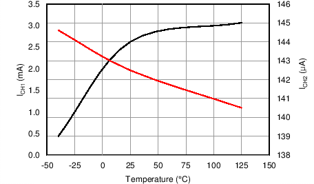
| ICH1 | Startup current with VDD shorted to GND | VVDD < 250 mV, VDRAIN = 100 V | –300 | –100 | µA | |
| ICH2 | Sourced current for startup at high VDD | VVDD = 8 V, VDRAIN = 100 V | –9.75 | –0.40 | mA | |
| ICH3 | Sourced current for startup at low VDD | VVDD = 2 V, VDRAIN = 100 V | –13.75 | –1.30 | mA | |
| VS INPUT | ||||||
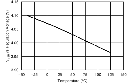
| VVSR | Regulating level | Measured in no load condition, TJ = 25°C |
4.01 | 4.05 | 4.09 | V |
| VVSNC | Negative clamp level | IVS = –300 μA, | –190 | –250 | –325 | mV |
| IVS | Input bias current | VVS = 4 V | –0.25 | 0.00 | 0.25 | µA |
| PROTECTION | ||||||
| IDOCP | DRAIN over current | IPK terminal shorted to GND | 0.725 | 0.850 | 0.925 | A |
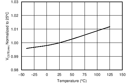
| VCSTE_OCP | Equivalent VCST(OCP) | VVS = 3.9 V, ID(ocp) x RIPK | 670 | 770 | 830 | V |
| VCSTE_OCP2 | Equivalent VCST(OCP2) | VVS = 3.9 V, ID(ocp2) x RIPK | 1200 | V | ||
| tONMAX(max) | Maximum FET on time at high load | VVS < 3.9 V, IPK shorted to GND | 13 | 18 | 24 | µs |
| tONMAX(min) | Maximum FET on time at low load | VVS > 4.1 V, IPK shorted to GND | 4.3 | 6 | 10 | µs |
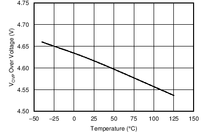
| VOVP | Over-voltage threshold | At VS input, TJ = 25°C | 4.45 | 4.60 | 4.75 | V |
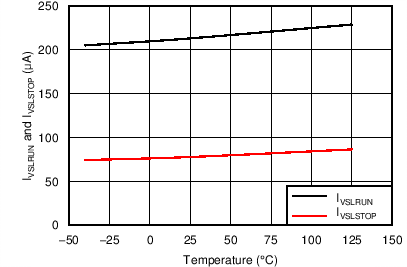
| IVSLRUN | VS line sense run current | Current out of VS terminal – increasing | 175 | 215 | 260 | µA |
| IVSLSTOP | VS line sense stop current | Current out of VS terminal – decreasing | 60 | 75 | 100 | µA |
| KVSL | Line sense IVS ratio | IVSL(run) / IVSL(stop) | 2.55 | 2.70 | 2.90 | A/A |
| VDDCLP | VDD voltage clamp | IVDDCLP forced = 2 mA | 26 | 28 | 30 | V |
| IVDDCLP_OC | VDD clamp over current | VVDD > 25 V | 4.65 | 6.00 | 7.65 | mA |
| TJ(stop) | Thermal shutdown temperature | Internal junction temperature | 150 | °C | ||
| TJ(hys) | Thermal shutdown hysteresis | Internal junction temperature | 50 | °C | ||
| POWER FET | ||||||
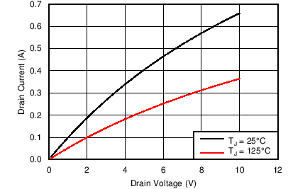
| BVDSS | Break-down voltage | TJ = 25°C | 700 | V | ||
| RDS(on) | Power FET on resistance | ID = 150 mA, TJ = 25°C | 10.5 | 12.0 | Ω | |
| ID = 150 mA, TJ = 125°C | 18.4 | 21.5 | Ω | |||
| ILEAKAGE | DRAIN terminal leakage current | VDS = 400 V HV, VS = 4.2 V DC TJ = 25°C |
10 | µA | ||
| VDS = 400 V HV, VS = 4.2 V DC TJ = 125°C |
20 | µA | ||||
| VDS = 700 V HV, VS = 4.2 V DC TJ = 25°C |
10 | µA | ||||
| CURRENTS | ||||||
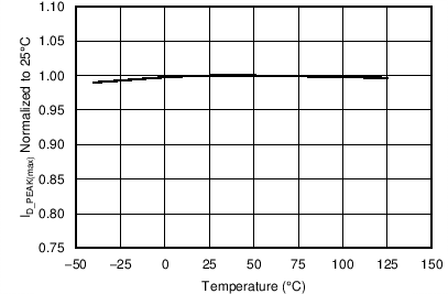
| ID_PEAK(max) | Maximum DRAIN peak current | VVDD = 15 V, IPK terminal shorted to GND, TJ = 25°C | 582 | 600 | 618 | mA |
| RIPK_SHORT | IPK to GND resistance Max to assume IPK shorted to GND | VVDD = 15 V | 200 | Ω | ||
| RIPK(min) | IPK to GND minimum resistance | VVDD = 15 V | 900 | Ω | ||
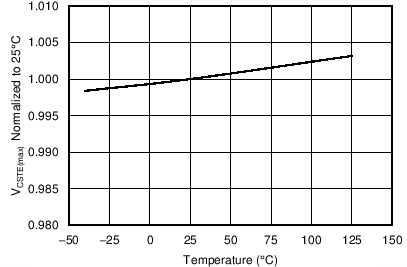
| VCSTE(max) | Equivalent current sense threshold | VVDD = 15 V, VVS = 3.9 V, ID_PK(max) × RIPK , TJ = 25°C | 532 | 540 | 548 | V |
| VCSTE(min) | Equivalent current sense threshold | VVDD = 15 V, VVS = 4.1 V, ID_PK(min) × RIPK | 160 | 180 | 200 | V |
| KAM | AM control ratio | VCSE(max) / VCSE(min) | 2.30 | 3.00 | 3.50 | V/V |
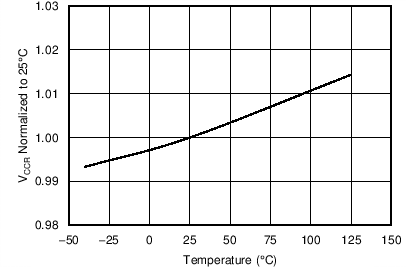
| KCC | CC regulation gain | VVDD = 15 V, VVS > 3.9 V; tDEMAG × fSW | 0.413 | |||
| VCCR | CC regulation constant | VVDD = 15 V, VVS < 3.9 V, VCSET(max) × KCC, TJ = 25°C | 216 | 223 | 230 | V |
7.7 Switching Characteristics
over operating free-air temperature range (unless otherwise noted)| PARAMETER | TEST CONDITIONS | MIN | TYP | MAX | UNIT | |
|---|---|---|---|---|---|---|
| TIMING | ||||||
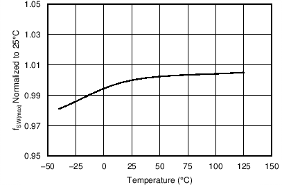
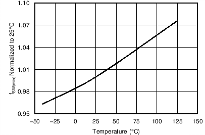
| fSW(max) | Maximum switching frequency | VVS < 3.9 V | 105 | 115 | 125 | kHz |
| fSW(min) | Minimum switching frequency | VVS > 4.1 V | 360 | 420 | 490 | Hz |
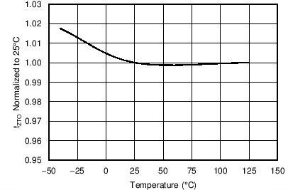
| tZTO | Zero crossing timeout delay | VVS < 3.9 V | 1.80 | 2.10 | 2.65 | µs |
| tON(min) | Minimum on time | IPK = 0.85 V | 390 | ns | ||
7.8 Typical Characteristics
Unless otherwise specified, VVDD = 15 V, TA = –40°C to 125°C, TA = TJ