ZHCSCD4B July 2013 – August 2014 UCC28910
PRODUCTION DATA.
- 1 特性
- 2 应用范围
- 3 说明
- 4 简化电路原理图 简化电路原理图
- 5 修订历史记录
- 6 Terminal Configuration and Functions
- 7 Specifications
-
8 Detailed Description
- 8.1 Overview
- 8.2 Functional Block Diagram
- 8.3 Detailed Device Description
- 8.4 Feature Description
- 8.5 Device Functional Modes
-
9 Applications and Implementation
- 9.1 Application Information
- 9.2
Typical Application
- 9.2.1
Battery Charger, 5 V, 6 W
- 9.2.1.1 Design Requirements
- 9.2.1.2
Detailed Design Procedure
- 9.2.1.2.1 Power Handling Curves
- 9.2.1.2.2 Definition of Terms
- 9.2.1.2.3 Maximum Target Switching Frequency
- 9.2.1.2.4 Transformer Turns Ratio, Inductance, Primary-Peak Current
- 9.2.1.2.5 Bulk Capacitance
- 9.2.1.2.6 Output Capacitance
- 9.2.1.2.7 VDD Capacitance, CVDD
- 9.2.1.2.8 VS Resistor Divider
- 9.2.1.2.9 RVDD Resistor and Turn Ratio
- 9.2.1.2.10 Transformer Input Power
- 9.2.1.2.11 RIPK Value
- 9.2.1.2.12 Primary Inductance Value
- 9.2.1.2.13 Pre-Load
- 9.2.1.2.14 DRAIN Voltage Clamp Circuit
- 9.2.1.3 Application Curves
- 9.2.1.4 Average Efficiency Performance and Standby Power of the UCC28910FBEVM-526
- 9.2.1
Battery Charger, 5 V, 6 W
- 10Power Supply Recommendations
- 11Layout
- 12器件和文档支持
- 13机械封装和可订购信息
6 Terminal Configuration and Functions
D (SOIC) PACKAGE
7 TERMINALS
(TOP VIEW)
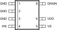
Terminal Functions
| TERMINAL | I/O | DESCRIPTION | |
|---|---|---|---|
| NAME | NO. | ||
| GND | 1, 2, 3 | G | The ground terminals (GND) are both the reference terminals for the controller and the low-side return for the drive output. Special care should be taken to return all AC decoupling as close as possible to this terminal and avoid any common trace length with analog signal return paths. |
| IPK | 4 | I | IPK is used to set the maximum peak current flowing in the power FET that is proportional to the maximum output current. |
| VS | 5 | I | Voltage Sense (VS) is used to provide voltage and timing feedback to the controller. Normally this terminal is connected to a voltage divider between an auxiliary winding and ground. The value of the upper resistor of this divider is used to program low line thresholds. |
| VDD | 6 | P | VDD is the supply terminal to the controller. A carefully placed bypass capacitor to GND is required on this terminal. |
| N/A | 7 | N/A | This pin is not present to provide enough distance between high voltage terminal (DRAIN) and the other pins |
| DRAIN | 8 | P | DRAIN, the drain of the internal power FET, but also the input for the high-voltage current source used to start up the device. |