ZHCSCD4B July 2013 – August 2014 UCC28910
PRODUCTION DATA.
- 1 特性
- 2 应用范围
- 3 说明
- 4 简化电路原理图 简化电路原理图
- 5 修订历史记录
- 6 Terminal Configuration and Functions
- 7 Specifications
-
8 Detailed Description
- 8.1 Overview
- 8.2 Functional Block Diagram
- 8.3 Detailed Device Description
- 8.4 Feature Description
- 8.5 Device Functional Modes
-
9 Applications and Implementation
- 9.1 Application Information
- 9.2
Typical Application
- 9.2.1
Battery Charger, 5 V, 6 W
- 9.2.1.1 Design Requirements
- 9.2.1.2
Detailed Design Procedure
- 9.2.1.2.1 Power Handling Curves
- 9.2.1.2.2 Definition of Terms
- 9.2.1.2.3 Maximum Target Switching Frequency
- 9.2.1.2.4 Transformer Turns Ratio, Inductance, Primary-Peak Current
- 9.2.1.2.5 Bulk Capacitance
- 9.2.1.2.6 Output Capacitance
- 9.2.1.2.7 VDD Capacitance, CVDD
- 9.2.1.2.8 VS Resistor Divider
- 9.2.1.2.9 RVDD Resistor and Turn Ratio
- 9.2.1.2.10 Transformer Input Power
- 9.2.1.2.11 RIPK Value
- 9.2.1.2.12 Primary Inductance Value
- 9.2.1.2.13 Pre-Load
- 9.2.1.2.14 DRAIN Voltage Clamp Circuit
- 9.2.1.3 Application Curves
- 9.2.1.4 Average Efficiency Performance and Standby Power of the UCC28910FBEVM-526
- 9.2.1
Battery Charger, 5 V, 6 W
- 10Power Supply Recommendations
- 11Layout
- 12器件和文档支持
- 13机械封装和可订购信息
11 Layout
11.1 Layout Guidelines
In order to increase the reliability and feasibility of the project it is recommended to follow the here below guidelines.
- Place the RIPK resistance as close as possible to the device with the shortest available traces.
- Try to minimize the area of DRAIN trace, this helps in keeping EMI disturbance low.
- A copper area connected to the GND terminals improves heat sinking thermal performance.
- A copper area connected to anode and cathode secondary diode improves heat sinking with an emphasis on the quiet area of the diode, the diode connected to the output capacitor, this limits the EMI disturbance.
- Place the auxiliary voltage sense resistor divider (RS1 and RS2 in Figure 41) directly on the VS pin keeping traces as short as possible.
11.2 Layout Example
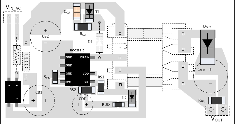 Figure 41. UCC28910 Layout Example